|
数据搜索系统,热门电子元器件搜索 |
|
|
数据搜索系统,热门电子元器件搜索 |
|
STDRIVE102BHTR 数据表(PDF) 19 Page - STMicroelectronics |
|
|
|||||||||||||||||||||||||||||
STDRIVE102BHTR 数据表(HTML) 19 Page - STMicroelectronics |
|
|
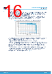
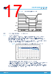
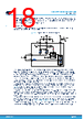
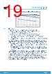
19 / 56 page  Figure 10. Charge pump output voltage with respect to the load current 0 2 4 6 8 10 12 14 0 5 10 15 20 25 30 35 Load Current [mA] VS = VM = VCC = 7 V VS = VM = VCC = 12 V VS = VM > 15 V 5.2 Gate drivers The gate drivers use a constant-current approach enabling the following advantages: • No external components are required between the MOSFETs’ gates and the drivers. • The slew rate of the half-bridge outputs is better controlled. The high-side drivers (Figure 11) and the low-side drivers (Figure 12) have a similar structure: • A reference pin for the low level (OUTx for the high-side and SLSx for the low-side). • The output pin (GHSx for the high-side or GLSx for the low-side), which directly drives the external MOSFET’s gate. • The supply pin (VBOOT in common to the three high side drivers and VCC in common to the three low side drivers). When the driver is not operative (for example, in standby mode or for very low supply), an equivalent 100 kΩ resistor keeps the external MOSFETs off. In normal conditions, the gate driver must force a voltage on the gate of its respective MOSFET, in order to keep it in a well-defined state. This datasheet adopts the following definitions: • Setting HIGH the gate driver means that the driver sources a controlled current to increase the VGS of the MOSFET and turn it on. The gate current comes from the supply VCC in case of the low-side driver or from VBOOT in case of the high-side driver. • Setting LOW the gate driver means that the driver sinks a controlled current from the gate of the MOSFET to turn it off. The sink circuitry of the driver is referred to the OUTx pin for the high-side, and to the SLSx pin for the low-side. This approach ensures that the MOSFET is kept off, even in the presence of below-GND transients. In normal mode operation, when a high-side driver is set HIGH, the voltage on the GHSx pin increases up to its target level VBOOT . At the same time the OUTx voltage increases up to VM, so that the VGS of the external MOSFET is kept under control (less or equal to VCC). In case the OUTx pin cannot follow the GHSx pin, the gate driver protects the gate of the external MOSFET from breakdown clamping the VGS at VGS, clamp. The six gate drivers (three low-side and three high-side) are controlled by six digital inputs, INH1/IN1, INH2/IN2, INH3/IN3, INL1/EN1, INL2/EN2, INL3/EN3. Each digital input has an internal pull-down resistor RPD,in. Each half- bridge (driven by a low-side driver and a high-side driver) is controlled by a couple of inputs: for example, INH1/IN1 and INL1/EN1 refer to half-bridge 1. The label INHx/INx or INLx/ENx can be used to indicate one of the three half-bridges, with no specific reference to a particular channel. Note that the terms “channel” or “phase” could be used similarly to refer to the half-bridge output. STDRIVE102BH, STDRIVE102H Device description DS14545 - Rev 1 page 19/56 |
|
链接网址 |
| ALLDATASHEET是否为您带来帮助? [ DONATE ] |
关于 Alldatasheet | 广告服务 | 联系我们 | 隐私政策 | 数据表链接 | 链接交换 | 制造商名单 All Rights Reserved©Alldatasheet.com |
| Russian : Alldatasheetru.com | Korean : Alldatasheet.co.kr | Spanish : Alldatasheet.es | French : Alldatasheet.fr | Italian : Alldatasheetit.com Portuguese : Alldatasheetpt.com | Polish : Alldatasheet.pl | Vietnamese : Alldatasheet.vn Indian : Alldatasheet.in | Mexican : Alldatasheet.com.mx | British : Alldatasheet.co.uk | New Zealand : Alldatasheet.co.nz |
|
Family Site : ic2ic.com |
icmetro.com |
 Chinese ▼
 English
 Chinese
 German
 Japanese
 Russian
 Korean
 Spanish
 French
 Italian
 Portuguese
 Polish
 Vietnamese
 Indian
 Mexican
 British
 New Zealand