|
数据搜索系统,热门电子元器件搜索 |
|
|
数据搜索系统,热门电子元器件搜索 |
|
ADV3003ACPZ-R7 数据表(PDF) 13 Page - Analog Devices |
|
|
|||||||||||||||||||||||||||||
ADV3003ACPZ-R7 数据表(HTML) 13 Page - Analog Devices |
|
|
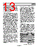
13 / 16 page  ADV3003 Rev. 0 | Page 13 of 16 The ADV3003 buffers the TMDS signals; therefore, the input traces can be considered electrically independent of the output traces. In most applications, the quality of the signal on the input TMDS traces is more sensitive to the PCB layout. Regardless of the data being carried on a specific TMDS channel, or whether the TMDS line is at the input or the output of the ADV3003, all four high speed signals should be routed on a PCB in accordance with the same RF layout guidelines. Layout for the TMDS Signals The TMDS differential pairs can either be microstrip traces, routed on the outer layer of a board, or stripline traces, routed on an internal layer of the board. If microstrip traces are used, there should be a continuous reference plane on the PCB layer directly below the traces. If stripline traces are used, they must be sandwiched between two continuous reference planes in the PCB stack-up. Additionally, the p and n of each differential pair must have a controlled differential impedance of 100 Ω. The characteristic impedance of a differential pair is a function of several variables including the trace width, the distance separating the two traces, the spacing between the traces and the reference plane, and the dielectric constant of the PC board binder material. Interlayer vias introduce impedance discontinuities that can cause reflections and jitter on the signal path; therefore, it is preferable to route the TMDS lines exclusively on one layer of the board, particularly for the input traces. In addition, to prevent unwanted signal coupling and interference, route the TMDS signals away from other signals and noise sources on the PCB. Both traces of a given differential pair must be equal in length to minimize intrapair skew. Maintaining the physical symmetry of a differential pair is integral to ensuring its signal integrity; excessive intrapair skew can introduce jitter through duty cycle distortion (DCD). The p and n of a given differential pair should always be routed together to establish the required 100 Ω differential impedance. Enough space should be left between the differential pairs of a given group so that the n of one pair does not couple to the p of another pair. For example, one tech- nique is to make the interpair distance 4× to 10× wider than the intrapair spacing. Any group of four TMDS channels (input or output) should have closely matched trace lengths to minimize interpair skew. Severe interpair skew can cause the data on the four different channels of a group to arrive out of alignment with one another. A good practice is to match the trace lengths for a given group of four channels to within 0.05 inches on FR4 material. The length of the TMDS traces should be minimized to reduce overall signal degradation. Commonly used PC board material such as FR4 is lossy at high frequencies, so long traces on the circuit board increase signal attenuation, resulting in decreased signal swing and increased jitter through intersymbol interference (ISI). Controlling the Characteristic Impedance of a TMDS Differential Pair The characteristic impedance of a differential pair depends on a number of variables including the trace width, the distance between the two traces, the height of the dielectric material between the trace and the reference plane below it, and the dielectric constant of the PCB binder material. To a lesser extent, the characteristic impedance also depends upon the trace thickness and the presence of solder mask. Many combinations can produce the correct characteristic imped- ance. It is generally required to work with the PC board fabri- cator to obtain a set of parameters to produce the desired results. One consideration is how to guarantee a differential pair with a differential impedance of 100 Ω over the entire length of the trace. One technique to accomplish this is to change the width of the traces in a differential pair based on how closely one trace is coupled to the other. When the two traces of a differential pair are close and strongly coupled, they should have a width that produces a 100 Ω differential impedance. When the traces split apart, for example, to go into a connector, and are no longer so strongly coupled, the width of the traces should be increased to yield a differential impedance of 100 Ω in the new configuration. Ground Current Return In some applications, it may be necessary to invert the output pin order of the ADV3003. This requires routing of the TMDS traces on multiple layers of the PCB. When routing differential pairs on multiple layers, it is also necessary to reroute the corres- ponding reference plane to provide one continuous ground current return path for the differential signals. Standard plated through-hole vias are acceptable for both the TMDS traces and the reference plane. An example of this routing is illustrated in Figure 27. To lower the impedance between the two ground planes, additional through-hole vias should be used to stitch the planes together, as space allows. PCB DIELECTRIC SILKSCREEN SILKSCREEN PCB DIELECTRIC PCB DIELECTRIC LAYER 2: GND (REFERENCE PLANE) LAYER 4: SIGNAL (MICROSTRIP) THROUGH-HOLE VIAS LAYER 1: SIGNAL (MICROSTRIP) KEEP REFERENCE PLANE ADJACENT TO SIGNAL ON ALL LAYERS TO PROVIDE CONTINUOUS GROUND CURRENT RETURN PATH. LAYER 3: PWR (REFERENCE PLANE) Figure 27. Example Routing of Reference Plane |
|
|
链接网址 |
| ALLDATASHEET是否为您带来帮助? [ DONATE ] |
关于 Alldatasheet | 广告服务 | 联系我们 | 隐私政策 | 数据表链接 | 链接交换 | 制造商名单 All Rights Reserved©Alldatasheet.com |
| Russian : Alldatasheetru.com | Korean : Alldatasheet.co.kr | Spanish : Alldatasheet.es | French : Alldatasheet.fr | Italian : Alldatasheetit.com Portuguese : Alldatasheetpt.com | Polish : Alldatasheet.pl | Vietnamese : Alldatasheet.vn Indian : Alldatasheet.in | Mexican : Alldatasheet.com.mx | British : Alldatasheet.co.uk | New Zealand : Alldatasheet.co.nz |
|
Family Site : ic2ic.com |
icmetro.com |
 Chinese ▼
 English
 Chinese
 German
 Japanese
 Russian
 Korean
 Spanish
 French
 Italian
 Portuguese
 Polish
 Vietnamese
 Indian
 Mexican
 British
 New Zealand