|
数据搜索系统,热门电子元器件搜索 |
|
|
数据搜索系统,热门电子元器件搜索 |
|
ADV3003ACPZ-R7 数据表(PDF) 14 Page - Analog Devices |
|
|
|||||||||||||||||||||||||||||
ADV3003ACPZ-R7 数据表(HTML) 14 Page - Analog Devices |
|
|
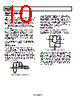
14 / 16 page  ADV3003 Rev. 0 | Page 14 of 16 TMDS Terminations In a typical application, all pins labeled AVEE, including the ePAD, should be connected directly to ground. All pins labeled AVCC, VTTI, or VTTO should be connected to 3.3 V. The supplies can also be powered individually, but care must be taken to ensure that each stage of the ADV3003 is powered correctly. The ADV3003 provides internal 50 Ω single-ended terminations for all its high speed inputs and outputs. The output termination resistors are always enabled and act to back-terminate the output TMDS transmission lines. These back-terminations act to absorb reflections from impedance discontinuities on the output traces, improving the signal integrity of the output traces and adding flexibility to how the output traces can be routed. For example, interlayer vias can be used to route the ADV3003 TMDS outputs on multiple layers of the PCB without severely degrading the quality of the output signal. Power Supply Bypassing The ADV3003 requires minimal supply bypassing. When powering the supplies individually, place a 0.01 μF capacitor between each 3.3 V supply pin (AVCC, VTTI, and VTTO) and ground to filter out supply noise. Generally, bypass capacitors should be placed near the power pins and should connect directly to the relevant supplies (without long intervening traces). For example, to improve the parasitic inductance of the power supply decoupling capacitors, minimize the trace length between capacitor landing pads and the vias as shown in Figure 28. In a typical application, the ADV3003 output is connected to an HDMI/DVI receiver or another device with a 50 Ω single-ended input termination. It is recommended that the outputs be terminated with external 50 Ω on-board resistors when the ADV3003 is not connected to another device. EXTRA ADDED INDUCTANCE RECOMMENDED NOT RECOMMENDED Auxiliary Control Signals There are four low-speed, single-ended control signals asso- ciated with each source or sink in an HDMI/DVI application. These control signals are hot plug detect (HPD), consumer electronics control (CEC), and two display data channel (DDC) lines. The two signals on the DDC bus are serial data and serial clock (SDA and SCL, respectively). The ADV3003, which is a TMDS-only part, does not buffer these low speed signals. If the end application requires it, use other means to buffer these signals. Figure 28. Recommended Pad Outline for Bypass Capacitors Power Supplies In applications where the ADV3003 is powered by a single 3.3 V supply, it is recommended to use two reference supply planes and bypass the 3.3 V reference plane to the ground reference plane with one 220 pF, one 1000 pF, two 0.01 μF, and one 4.7 μF capacitors. The capacitors should via down directly to the supply planes and be placed within a few centimeters of the ADV3003. The ADV3003 has three separate power supplies referenced to a single ground, AVEE. The supply/ground pairs are as follows: AVCC/AVEE, VTTI/AVEE, and VTTO/AVEE. The AVCC/AVEE supply (3.3 V) powers the core of the ADV3003. The VTTI/AVEE supply (3.3 V) powers the input termination (see Figure 25). Similarly, the VTTO/AVEE supply (3.3 V) powers the output termination (see Figure 26). |
|
|
链接网址 |
| ALLDATASHEET是否为您带来帮助? [ DONATE ] |
关于 Alldatasheet | 广告服务 | 联系我们 | 隐私政策 | 数据表链接 | 链接交换 | 制造商名单 All Rights Reserved©Alldatasheet.com |
| Russian : Alldatasheetru.com | Korean : Alldatasheet.co.kr | Spanish : Alldatasheet.es | French : Alldatasheet.fr | Italian : Alldatasheetit.com Portuguese : Alldatasheetpt.com | Polish : Alldatasheet.pl | Vietnamese : Alldatasheet.vn Indian : Alldatasheet.in | Mexican : Alldatasheet.com.mx | British : Alldatasheet.co.uk | New Zealand : Alldatasheet.co.nz |
|
Family Site : ic2ic.com |
icmetro.com |
 Chinese ▼
 English
 Chinese
 German
 Japanese
 Russian
 Korean
 Spanish
 French
 Italian
 Portuguese
 Polish
 Vietnamese
 Indian
 Mexican
 British
 New Zealand