|
数据搜索系统,热门电子元器件搜索 |
|
|
数据搜索系统,热门电子元器件搜索 |
|
OP1177ARMZ-R2 数据表(PDF) 14 Page - Analog Devices |
|
|
|||||||||||||||||||||||||||||
OP1177ARMZ-R2 数据表(HTML) 14 Page - Analog Devices |
|
|
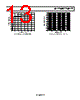
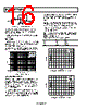
14 / 24 page  OP1177/OP2177/OP4177 Rev. E | Page 14 of 24 FUNCTIONAL DESCRIPTION The OPx177 series is the fourth generation of Analog Devices, Inc., industry-standard OP07 amplifier family. OPx177 is a high precision, low noise operational amplifier with a combination of extremely low offset voltage and very low input bias currents. Unlike JFET amplifiers, the low bias and offset currents are relatively insensitive to ambient temperatures, even up to 125°C. Analog Devices proprietary process technology and linear design expertise has produced a high voltage amplifier with superior performance to the OP07, OP77, and OP177 in a tiny MSOP 8lead package. Despite its small size, the OPx177 offers numerous improvements, including low wideband noise, very wide input and output voltage range, lower input bias current, and complete freedom from phase inversion. OPx177 has a specified operating temperature range as wide as any similar device in a plastic surface-mount package. This is increasingly important as PCB and overall system sizes continue to shrink, causing internal system temperatures to rise. Power consumption is reduced by a factor of four from the OP177, and bandwidth and slew rate increase by a factor of two. The low power dissipation and very stable performance vs. temperature also act to reduce warmup drift errors to insignificant levels. Open-loop gain linearity under heavy loads is superior to compet- itive parts, such as the OPA277, improving dc accuracy and reducing distortion in circuits with high closed-loop gains. Inputs are internally protected from overvoltage conditions referenced to either supply rail. Like any high performance amplifier, maximum performance is achieved by following appropriate circuit and PCB guidelines. The following sections provide practical advice on getting the most out of the OPx177 under a variety of application conditions. TOTAL NOISE-INCLUDING SOURCE RESISTORS The low input current noise and input bias current of the OPx177 make it useful for circuits with substantial input source resistance. Input offset voltage increases by less than 1 μV maximum per 500 Ω of source resistance. The total noise density of the OPx177 is () S S n n TOTAL n kTR R i e e 4 2 2 , + + = where: en is the input voltage noise density. in is the input current noise density. RS is the source resistance at the noninverting terminal. k is Boltzmann’s constant (1.38 × 10⁻²³ J/K). T is the ambient temperature in Kelvin (T = 273 + temperature in degrees Celsius). For RS < 3.9 kΩ, en dominates and en,TOTAL ≈ en For 3.9 kΩ < RS < 412 kΩ, voltage noise of the amplifier, the current noise of the amplifier translated through the source resistor, and the thermal noise from the source resistor all contribute to the total noise. For RS > 412 kΩ, the current noise dominates and en,TOTAL ≈ inRS The total equivalent rms noise over a specific bandwidth is expressed as ( ) BW e e TOTAL n n , = where BW is the bandwidth in hertz. The preceding analysis is valid for frequencies larger than 50 Hz. When considering lower frequencies, flicker noise (also known as 1/f noise) must be taken into account. For a reference on noise calculations, refer to the Band-Pass KRC or Sallen-Key Filter section. GAIN LINEARITY Gain linearity reduces errors in closed-loop configurations. The straighter the gain curve, the lower the maximum error over the input signal range. This is especially true for circuits with high closed-loop gains. The OP1177 has excellent gain linearity even with heavy loads, as shown in Figure 51. Compare its performance to the OPA277, shown in Figure 52. Both devices are measured under identical conditions, with RL = 2 kΩ. The OP2177 (dual) has virtually no distortion at lower voltages. Compared to the OPA277 at several supply voltages and various loads, OP1177 performance far exceeds that of its counterpart. (5V/DIV) OP1177 VSY = ±15V RL = 2kΩ Figure 51. Gain Linearity |
|
|
链接网址 |
| ALLDATASHEET是否为您带来帮助? [ DONATE ] |
关于 Alldatasheet | 广告服务 | 联系我们 | 隐私政策 | 数据表链接 | 链接交换 | 制造商名单 All Rights Reserved©Alldatasheet.com |
| Russian : Alldatasheetru.com | Korean : Alldatasheet.co.kr | Spanish : Alldatasheet.es | French : Alldatasheet.fr | Italian : Alldatasheetit.com Portuguese : Alldatasheetpt.com | Polish : Alldatasheet.pl | Vietnamese : Alldatasheet.vn Indian : Alldatasheet.in | Mexican : Alldatasheet.com.mx | British : Alldatasheet.co.uk | New Zealand : Alldatasheet.co.nz |
|
Family Site : ic2ic.com |
icmetro.com |
 Chinese ▼
 English
 Chinese
 German
 Japanese
 Russian
 Korean
 Spanish
 French
 Italian
 Portuguese
 Polish
 Vietnamese
 Indian
 Mexican
 British
 New Zealand