|
数据搜索系统,热门电子元器件搜索 |
|
|
数据搜索系统,热门电子元器件搜索 |
|
OP1177ARMZ-R2 数据表(PDF) 17 Page - Analog Devices |
|
|
|||||||||||||||||||||||||||||
OP1177ARMZ-R2 数据表(HTML) 17 Page - Analog Devices |
|
|
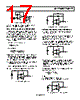
17 / 24 page  OP1177/OP2177/OP4177 Rev. E | Page 17 of 24 OP1177 6 7 2 3 4 V+ V– VOUT RS + – 400mV CS CL Figure 58. Snubber Network Configuration Caution: The snubber technique cannot recover the loss of bandwidth induced by large capacitive loads. STRAY INPUT CAPACITANCE COMPENSATION The effective input capacitance in an operational amplifier circuit (Ct) consists of three components. These are the internal differential capacitance between the input terminals, the internal common-mode capacitance of each input to ground, and the external capacitance including parasitic capacitance. In the circuit in Figure 59, the closed-loop gain increases as the signal frequency increases. The transfer function of the circuit is () R1 sC R1 R2 t + + 1 1 indicating a zero at () t t C R2 R1 R2R1C R1 R2 s / 2 1 π = + = Depending on the value of R1 and R2, the cutoff frequency of the closed-loop gain can be well below the crossover frequency. In this case, the phase margin (ΦM) can be severely degraded, resulting in excessive ringing or even oscillation. A simple way to overcome this problem is to insert a capacitor in the feedback path, as shown in Figure 60. The resulting pole can be positioned to adjust the phase margin. Setting Cf = (R1/R2) Ct achieves a phase margin of 90°. R2 R1 V1 + – OP1177 2 3 VOUT Ct 6 7 4 V+ V– Figure 59. Stray Input Capacitance R2 R1 V1 + – OP1177 2 3 VOUT Ct Cf 6 7 4 V+ V– Figure 60. Compensation Using Feedback Capacitor REDUCING ELECTROMAGNETIC INTERFERENCE A number of methods can be utilized to reduce the effects of EMI on amplifier circuits. In one method, stray signals on either input are coupled to the opposite input of the amplifier. The result is that the signal is rejected according to the CMRR of the amplifier. This is usually achieved by inserting a capacitor between the inputs of the amplifier, as shown in Figure 61. However, this method can also cause instability, depending on the value of capacitance. R2 R1 V1 + – OP1177 2 3 VOUT C 6 7 4 V+ V– Figure 61. EMI Reduction Placing a resistor in series with the capacitor (see Figure 62) increases the dc loop gain and reduces the output error. Positioning the breakpoint (introduced by R-C) below the secondary pole of the operational amplifier improves the phase margin and, therefore, stability. R can be chosen independently of C for a specific phase margin according to the formula () ⎟ ⎠ ⎞ ⎜ ⎝ ⎛ + − = R1 R2 jf a R2 R 2 1 where: a is the open-loop gain of the amplifier. f2 is the frequency at which the phase of a = ΦM − 180°. OP1177 2 3 R C R1 R2 VOUT V1 + – 6 7 4 V+ V– Figure 62. Compensation Using Input R-C Network |
|
|
链接网址 |
| ALLDATASHEET是否为您带来帮助? [ DONATE ] |
关于 Alldatasheet | 广告服务 | 联系我们 | 隐私政策 | 数据表链接 | 链接交换 | 制造商名单 All Rights Reserved©Alldatasheet.com |
| Russian : Alldatasheetru.com | Korean : Alldatasheet.co.kr | Spanish : Alldatasheet.es | French : Alldatasheet.fr | Italian : Alldatasheetit.com Portuguese : Alldatasheetpt.com | Polish : Alldatasheet.pl | Vietnamese : Alldatasheet.vn Indian : Alldatasheet.in | Mexican : Alldatasheet.com.mx | British : Alldatasheet.co.uk | New Zealand : Alldatasheet.co.nz |
|
Family Site : ic2ic.com |
icmetro.com |
 Chinese ▼
 English
 Chinese
 German
 Japanese
 Russian
 Korean
 Spanish
 French
 Italian
 Portuguese
 Polish
 Vietnamese
 Indian
 Mexican
 British
 New Zealand