|
数据搜索系统,热门电子元器件搜索 |
|
|
数据搜索系统,热门电子元器件搜索 |
|
OP1177ARMZ-R2 数据表(PDF) 16 Page - Analog Devices |
|
|
|||||||||||||||||||||||||||||
OP1177ARMZ-R2 数据表(HTML) 16 Page - Analog Devices |
|
|
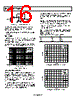
16 / 24 page  OP1177/OP2177/OP4177 Rev. E | Page 16 of 24 OP1177 6 7 2 3 4 V+ V– R2 100kΩ VOUT 10kΩ R1 1kΩ + – 200mV Figure 54. Test Circuit for Overload Recovery Time Figure 18 shows the positive overload recovery time of the OP1177. The output recovers in less than 4 μs after being overdriven by more than 100%. The negative overload recovery of the OP1177 is 1.4 μs, as seen in Figure 19. THD + NOISE The OPx177 has very low total harmonic distortion. This indicates excellent gain linearity and makes the OPx177 a great choice for high closed-loop gain precision circuits. Figure 55 shows that the OPx177 has approximately 0.00025% distortion in unity gain, the worst-case configuration for distortion. FREQUENCY (Hz) 100 1k 0.001 0.01 20 6k 0.0001 0.1 VSY = ±15V RL = 10kΩ BW = 22kHz Figure 55. THD + N vs. Frequency CAPACITIVE LOAD DRIVE OPx177 is inherently stable at all gains and capable of driving large capacitive loads without oscillation. With no external compensation, the OPx177 safely drives capacitive loads up to 1000 pF in any configuration. As with virtually any amplifier, driving larger capacitive loads in unity gain requires additional circuitry to assure stability. In this case, a snubber network is used to prevent oscillation and reduce the amount of overshoot. A significant advantage of this method is that it does not reduce the output swing because the Resistor RS is not inside the feedback loop. Figure 56 is a scope shot of the output of the OPx177 in response to a 400 mV pulse. The load capacitance is 2 nF. The circuit is configured in positive unity gain, the worst-case condition for stability. As shown in Figure 58, placing an R-C network parallel to the load capacitance (CL) allows the amplifier to drive higher values of CL without causing oscillation or excessive overshoot. There is no ringing, and overshoot is reduced from 27% to 5% using the snubber network. Optimum values for RS and CS are tabulated in Table 5 for several capacitive loads, up to 200 nF. Values for other capacitive loads can be determined experimentally. Table 5. Optimum Values for Capacitive Loads CL RS CS 10 nF 20 Ω 0.33 μF 50 nF 30 Ω 6.8 nF 200 nF 200 Ω 0.47 μF 0 GND TIME (10µs/DIV) VSY = ±5V RL = 10kΩ CL = 2nF Figure 56. Capacitive Load Drive Without Snubber GND TIME (10µs/DIV) VSY = ±5V RL = 10kΩ RS = 200Ω CL = 2nF CS = 0.47µF Figure 57. Capacitive Load Drive with Snubber |
|
|
链接网址 |
| ALLDATASHEET是否为您带来帮助? [ DONATE ] |
关于 Alldatasheet | 广告服务 | 联系我们 | 隐私政策 | 数据表链接 | 链接交换 | 制造商名单 All Rights Reserved©Alldatasheet.com |
| Russian : Alldatasheetru.com | Korean : Alldatasheet.co.kr | Spanish : Alldatasheet.es | French : Alldatasheet.fr | Italian : Alldatasheetit.com Portuguese : Alldatasheetpt.com | Polish : Alldatasheet.pl | Vietnamese : Alldatasheet.vn Indian : Alldatasheet.in | Mexican : Alldatasheet.com.mx | British : Alldatasheet.co.uk | New Zealand : Alldatasheet.co.nz |
|
Family Site : ic2ic.com |
icmetro.com |
 Chinese ▼
 English
 Chinese
 German
 Japanese
 Russian
 Korean
 Spanish
 French
 Italian
 Portuguese
 Polish
 Vietnamese
 Indian
 Mexican
 British
 New Zealand