|
数据搜索系统,热门电子元器件搜索 |
|
|
数据搜索系统,热门电子元器件搜索 |
|
AD8610ARM-R2 数据表(PDF) 15 Page - Analog Devices |
|
|
|||||||||||||||||||||||||||||
AD8610ARM-R2 数据表(HTML) 15 Page - Analog Devices |
|
|
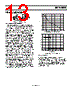
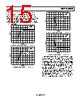
15 / 24 page  AD8610/AD8620 Slew Rate (Unity Gain Inverting vs. Noninverting) VS = ±13V RL = 2kΩ Amplifiers generally have a faster slew rate in an inverting unity G= –1 gain configuration due to the absence of the differential input SR = 54V/µs TIME (400ns/DIV) capacitance. Figure 49 through Figure 52 show the performance of the AD8610/AD8620 configured in a gain of –1 compared to the OPA627. The AD8610/AD8620 slew rate is more symmetrical, and both the positive and negative transitions are much cleaner than in the OPA627. V R S = ±13V L = 2kΩ G = –1 SR = 54V/µs Figure 51. –Slew Rate of AD8610/AD8620 in Unity Gain of –1 VS = ±13V RL = 2kΩ G= –1 SR = 56V/µs TIME (400ns/DIV) Figure 49. +Slew Rate of AD8610/AD8620 in Unity Gain of –1 VS = ±13V RL = 2kΩ G= –1 TIME (400ns/DIV) SR = 42.1V/µs Figure 52. –Slew Rate of OPA627 in Unity Gain of –1 The AD8610/AD8620 have a very fast slew rate of 60 V/μs even when configured in a noninverting gain of +1. This is the toughest condition to impose on any amplifier since the input common- mode capacitance of the amplifier generally makes its SR appear worse. The slew rate of an amplifier varies according to the voltage difference between its two inputs. To observe the maximum SR, a voltage difference of about 2 V between the inputs must be TIME (400ns/DIV) ensured. This is required for virtually any JFET op amp so that Figure 50. +Slew Rate of OPA627 in Unity Gain of –1 one side of the op amp input circuit is completely off, thus maxi mizing the current available to charge and discharge the internal compensation capacitance. Lower differential drive voltages produce lower slew rate readings. A JFET input op amp with a slew rate of 60 V/μs at unity gain with VIN = 10 V might slew at 20 V/μs, if it is operated at a gain of +100 with VIN = 100 mV. Rev. E | Page 15 of 24 |
|
|
链接网址 |
| ALLDATASHEET是否为您带来帮助? [ DONATE ] |
关于 Alldatasheet | 广告服务 | 联系我们 | 隐私政策 | 数据表链接 | 链接交换 | 制造商名单 All Rights Reserved©Alldatasheet.com |
| Russian : Alldatasheetru.com | Korean : Alldatasheet.co.kr | Spanish : Alldatasheet.es | French : Alldatasheet.fr | Italian : Alldatasheetit.com Portuguese : Alldatasheetpt.com | Polish : Alldatasheet.pl | Vietnamese : Alldatasheet.vn Indian : Alldatasheet.in | Mexican : Alldatasheet.com.mx | British : Alldatasheet.co.uk | New Zealand : Alldatasheet.co.nz |
|
Family Site : ic2ic.com |
icmetro.com |
 Chinese ▼
 English
 Chinese
 German
 Japanese
 Russian
 Korean
 Spanish
 French
 Italian
 Portuguese
 Polish
 Vietnamese
 Indian
 Mexican
 British
 New Zealand