|
数据搜索系统,热门电子元器件搜索 |
|
|
数据搜索系统,热门电子元器件搜索 |
|
AD8610ARM-R2 数据表(PDF) 16 Page - Analog Devices |
|
|
|||||||||||||||||||||||||||||
AD8610ARM-R2 数据表(HTML) 16 Page - Analog Devices |
|
|
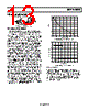
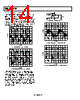
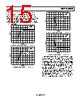
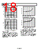
16 / 24 page  AD8610/AD8620 The slew rate of the AD8610/AD8620 is double that of the Input Overvoltage Protection OPA627 when configured in a unity gain of +1 (see Figure 53 When the input of an amplifier is driven below VEE or above and Figure 54). VCC by more than one VBE, large currents flow from the sub strate through the negative supply (V–) or the positive supply VS = ±13V RL = 2kΩ (V+), respectively, to the input pins and can destroy the device. G= +1 If the input source can deliver larger currents than the maximum forward current of the diode (>5 mA), a series resistor can be added to protect the inputs. With its very low input bias and offset current, a large series resistor can be placed in front of the AD8610/AD8620 inputs to limit current to below damaging SR = 85V/µs levels. Series resistance of 10 kΩ generates less than 25 μV of offset. This 10 kΩ allows input voltages more than 5 V beyond either power supply. Thermal noise generated by the resistor adds 7.5 nV/√Hz to the noise of the AD8610/AD8620. For the AD8610/ AD8620, differential voltages equal to the supply voltage do not cause any problem (see Figure 55). In this context, please note that TIME (400ns/DIV) the high breakdown voltage of the input FETs eliminates the need Figure 53. +Slew Rate of AD8610/AD8620 in Unity Gain of +1 to include clamp diodes between the inputs of the amplifier, a prac- VS = ±13V tice that is mandatory on many precision op amps. Unfortunately, RL = 2kΩ G= +1 clamp diodes greatly interfere with many application circuits such as precision rectifiers and comparators. The AD8610/ AD8620 are free from these limitations. +13V 3 7 6 2 –13V 4 AD8610 V1 14V SR = 23V/µs 0 Figure 56. Unity Gain Follower No Phase Reversal Many amplifiers misbehave when one or both of the inputs are TIME (400ns/DIV) Figure 54. +Slew Rate of OPA627 in Unity Gain of +1 forced beyond the input common-mode voltage range. Phase reversal is typified by the transfer function of the amplifier, effect- The slew rate of an amplifier determines the maximum frequency tively reversing its transfer polarity. In some cases, this can cause at which it can respond to a large signal input. This frequency lockup and even equipment damage in servo systems, and can (known as full-power bandwidth or FPBW) can be calculated cause permanent damage or no recoverable parameter shifts to for a given distortion (for example, 1%) from the equation: the amplifier itself. Many amplifiers feature compensation cir- SR cuitry to combat these effects, but some are only effective for FPBW = the inverting input. The AD8610/AD8620 are designed to prevent (2π ×V PEAK ) phase reversal when one or both inputs are forced beyond their input common-mode voltage range. CH1 = 20.8V p-p CH2 = 19.4V p-p VOUT VIN 0V 0V TIME (400ns/DIV) Figure 55. AD8610 FPBW TIME (400µs/DIV) Figure 57. No Phase Reversal Rev. E | Page 16 of 24 |
|
|
链接网址 |
| ALLDATASHEET是否为您带来帮助? [ DONATE ] |
关于 Alldatasheet | 广告服务 | 联系我们 | 隐私政策 | 数据表链接 | 链接交换 | 制造商名单 All Rights Reserved©Alldatasheet.com |
| Russian : Alldatasheetru.com | Korean : Alldatasheet.co.kr | Spanish : Alldatasheet.es | French : Alldatasheet.fr | Italian : Alldatasheetit.com Portuguese : Alldatasheetpt.com | Polish : Alldatasheet.pl | Vietnamese : Alldatasheet.vn Indian : Alldatasheet.in | Mexican : Alldatasheet.com.mx | British : Alldatasheet.co.uk | New Zealand : Alldatasheet.co.nz |
|
Family Site : ic2ic.com |
icmetro.com |
 Chinese ▼
 English
 Chinese
 German
 Japanese
 Russian
 Korean
 Spanish
 French
 Italian
 Portuguese
 Polish
 Vietnamese
 Indian
 Mexican
 British
 New Zealand