|
数据搜索系统,热门电子元器件搜索 |
|
|
数据搜索系统,热门电子元器件搜索 |
|
AD8610ARM-R2 数据表(PDF) 19 Page - Analog Devices |
|
|
|||||||||||||||||||||||||||||
AD8610ARM-R2 数据表(HTML) 19 Page - Analog Devices |
|
|
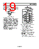
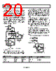
19 / 24 page  AD8610/AD8620 Rev. E | Page 19 of 24 Input Offset Voltage Adjustment Offset of AD8610 is very small and normally does not require additional offset adjustment. However, the offset adjust pins can be used as shown in Figure 66 to further reduce the dc offset. By using resistors in the range of 50 kΩ, offset trim range is ±3.3 mV. R1 +VS VOUT –VS AD8610 7 6 1 5 4 3 2 Figure 66. Offset Voltage Nulling Circuit Programmable Gain Amplifier (PGA) The combination of low noise, low input bias current, low input offset voltage, and low temperature drift make the AD8610/ AD8620 a perfect solution for programmable gain amplifiers. PGAs are often used immediately after sensors to increase the dynamic range of the measurement circuit. Historically, the large on resistance of switches (combined with the large IB currents of amplifiers) created a large dc offset in PGAs. Recent and improved monolithic switches and amplifiers completely remove these problems. A PGA discrete circuit is shown in Figure 67. In Figure 67, when the 10 pA bias current of the AD8610 is dropped across the (<5 Ω) RON of the switch, it results in a negligible offset error. When high precision resistors are used, as in the circuit of Figure 67, the error introduced by the PGA is within the ½ LSB requirement for a 16-bit system. VIN VOUT AD8610 7 4 6 5 1 2 3 IN1 S1 D1 10kΩ 10kΩ 1kΩ 5V +5V IN2 S2 D2 IN3 S3 D3 IN4 S4 D4 ADG452 3 2 14 15 11 10 6 7 VL VDD 13 12 1 16 9 8 74HC139 VSS 4 GND 5 1kΩ 100Ω 11Ω 5pF G = +1 G = +10 G = +100 G = +1000 +5V +5V –5V Y0 Y1 Y2 Y3 G A B A0 A1 100Ω Figure 67. High Precision PGA 1. Room temperature error calculation due to RON and IB: ΔVOS = IB × RON = 2 pA × 5 Ω = 10 pV Total Offset = AD8610 (Offset) + ΔVOS Total Offset = AD8610 (Offset_Trimmed) + ΔVOS μV 5 pV 10 μV 5 ≅ + = Offset Total 2. Full temperature error calculation due to RON and IB: ΔVOS (@ 85°C) = IB (@ 85°C) × RON (@ 85°C) = 250 pA × 15 Ω = 3.75 nV 3. Temperature coefficient of switch and AD8610/AD8620 combined is essentially the same as the TCVOS of the AD8610/AD8620: ΔVOS/ΔT(total) = ΔVOS/ΔT(AD8610/AD8620) + ΔVOS/ΔT(IB × RON) C V C C total T V OS ° μ ≅ ° + ° = Δ Δ / 5 . 0 nV/ 06 . 0 / μV 5 . 0 ) ( / |
|
|
链接网址 |
| ALLDATASHEET是否为您带来帮助? [ DONATE ] |
关于 Alldatasheet | 广告服务 | 联系我们 | 隐私政策 | 数据表链接 | 链接交换 | 制造商名单 All Rights Reserved©Alldatasheet.com |
| Russian : Alldatasheetru.com | Korean : Alldatasheet.co.kr | Spanish : Alldatasheet.es | French : Alldatasheet.fr | Italian : Alldatasheetit.com Portuguese : Alldatasheetpt.com | Polish : Alldatasheet.pl | Vietnamese : Alldatasheet.vn Indian : Alldatasheet.in | Mexican : Alldatasheet.com.mx | British : Alldatasheet.co.uk | New Zealand : Alldatasheet.co.nz |
|
Family Site : ic2ic.com |
icmetro.com |
 Chinese ▼
 English
 Chinese
 German
 Japanese
 Russian
 Korean
 Spanish
 French
 Italian
 Portuguese
 Polish
 Vietnamese
 Indian
 Mexican
 British
 New Zealand