|
数据搜索系统,热门电子元器件搜索 |
|
|
数据搜索系统,热门电子元器件搜索 |
|
AD8067ART-R2 数据表(PDF) 14 Page - Analog Devices |
|
|
|||||||||||||||||||||||||||||
AD8067ART-R2 数据表(HTML) 14 Page - Analog Devices |
|
|
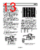
14 / 24 page  AD8067 Rev. A | Page 14 of 24 For inverting voltage gain applications, the source impedance of the input signal must be considered because it sets the application’s noise gain as well as the apparent closed-loop gain. The basic frequency equation for inverting applications is S G F S G R R R R R GBP equency p –3 dB Fr Closed-Loo + + + × = ) ( S G F R R R Gain DC + = – where GBP is the gain bandwidth product of the amplifier, and RS is the signal source resistance. S G S G F R R R R R Gain Noise ion Configurat Inverting + + + = It is important that the noise gain for inverting applications be kept above 6 for stability reasons. If the signal source driving the inverter is another amplifier, take care that the driving amplifier shows low output impedance through the frequency span of the expected closed-loop bandwidth of the AD8067. RESISTOR SELECTION FOR WIDEBAND OPERATION Voltage feedback amplifiers can use a wide range of resistor values to set their gain. Proper design of the application’s feedback network requires consideration of the following issues: • Poles formed by the amplifier’s input capacitances with the resistances seen at the amplifier’s input terminals • Effects of mismatched source impedances • Resistor value impact on the application’s output voltage noise • Amplifier loading effects The AD8067 has common-mode input capacitances (CM) of 1.5 pF and a differential input capacitance (CD) of 2.5 pF. This is illustrated in Figure 43. The source impedance driving the positive input of a noninverting buffer forms a pole primarily with the amplifier’s common-mode input capacitance as well as any parasitic capacitance due to the board layout (CPAR). This limits the obtainable bandwidth. For G = +10 buffers, this bandwidth limit becomes apparent for source impedances >1 kΩ. VI RS SIGNAL SOURCE – + – + VOUT – + CPAR CPAR RG CD CM CM RF Figure 43. Input and Board Capacitances There is a pole in the feedback loop response formed by the source impedance seen by the amplifier’s negative input (RG ⎢⎢RF) and the sum of the amplifier’s differential input capacitance, common-mode input capacitance, and any board parasitic capacitance. This decreases the loop phase margin and can cause stability problems, that is, unacceptable peaking and ringing in the response. To avoid this problem, it is recommended that the resistance at the AD8067’s negative input be kept below 200 Ω for all wideband voltage gain applications. Matching the impedances at the inputs of the AD8067 is also recommended for wideband voltage gain applications. This minimizes nonlinear common-mode capacitive effects that can significantly degrade settling time and distortion performance. The AD8067 has a low input voltage noise of 6.6 nV/√Hz. Source resistances greater than 500 Ω at either input terminal notably increases the apparent referred-to-input (RTI) voltage noise of the application. The amplifier must supply output current to its feedback network, as well as to the identified load. For instance, the load resistance presented to the amplifier in Figure 40 is RLOAD ⎪⎪ (RF + RG). For an RLOAD of 100 Ω, RF of 1 kΩ, and RG of 100 Ω, the amplifier is driving a total load resistance of about 92 Ω. This becomes more of an issue as RF decreases. The AD8067 is rated to provide 30 mA of low distortion output current. Heavy output drive requirements also increase the part’s power dissipation and should be taken into account. |
|
|
链接网址 |
| ALLDATASHEET是否为您带来帮助? [ DONATE ] |
关于 Alldatasheet | 广告服务 | 联系我们 | 隐私政策 | 数据表链接 | 链接交换 | 制造商名单 All Rights Reserved©Alldatasheet.com |
| Russian : Alldatasheetru.com | Korean : Alldatasheet.co.kr | Spanish : Alldatasheet.es | French : Alldatasheet.fr | Italian : Alldatasheetit.com Portuguese : Alldatasheetpt.com | Polish : Alldatasheet.pl | Vietnamese : Alldatasheet.vn Indian : Alldatasheet.in | Mexican : Alldatasheet.com.mx | British : Alldatasheet.co.uk | New Zealand : Alldatasheet.co.nz |
|
Family Site : ic2ic.com |
icmetro.com |
 Chinese ▼
 English
 Chinese
 German
 Japanese
 Russian
 Korean
 Spanish
 French
 Italian
 Portuguese
 Polish
 Vietnamese
 Indian
 Mexican
 British
 New Zealand