|
数据搜索系统,热门电子元器件搜索 |
|
|
数据搜索系统,热门电子元器件搜索 |
|
AD8571ARMZ-R2 数据表(PDF) 15 Page - Analog Devices |
|
|
|||||||||||||||||||||||||||||
AD8571ARMZ-R2 数据表(HTML) 15 Page - Analog Devices |
|
|
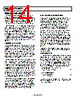
15 / 24 page  AD8571/AD8572/AD8574 Rev. C | Page 15 of 24 VIN+ VIN– VOUT AB AA ΦA1 ΦB VOSA + VOSB + BB CM2 CM1 ΦA2 VNB VNA –BA VOA ΦB variation or long-term wear time, both of which are much slower than the auto-zero clock frequency of the AD857x, which effectively makes the VOS time invariant, and Equation 5 can be rewritten as [] [ ] ( ) A OSA A A OSA A A IN A OA B V B A V B A t V A t V + − + + = 1 1 (6) or [] [ ] ⎟ ⎟ ⎠ ⎞ ⎜ ⎜ ⎝ ⎛ + + = A OSA IN A OA B V t V A t V 1 (7) Figure 50. Auto-Zero Phase of the Amplifier AMPLIFICATION PHASE Here, the auto-zeroing becomes apparent. Note that the VOS term is reduced by a 1 + B When the φB switches close and the φA switches open for the amplification phase, the offset voltage remains on C A factor, which shows how the nulling amplifier has greatly reduced its own offset voltage error even before correcting the primary amplifier. Therefore, the primary amplifier output voltage is the voltage at the output of the AD857x amplifier. It is equal to M1 and essentially corrects any error from the nulling amplifier. The voltage across CM1 is designated as VNA. The potential difference between the two inputs to the primary amplifier is designated as V , or V = (V − V IN IN IN+ IN– ). The output of the nulling amplifier can then be expressed as [ ] [ ] ( ) NB B OSB IN B OUT V B V t V A t V + + = (8) [] [] [ ] [] t V B t V t V A t V NA A OSA IN A OA − − = ( (3) = V , so this can be rewritten as In the amplification phase, VOA NB [ ] [] [] ⎥ ⎥ ⎦ ⎤ ⎢ ⎢ ⎣ ⎡ ⎟⎟ ⎠ ⎞ ⎜⎜ ⎝ ⎛ + + + + = A OSA IN A B OSB B IN B OUT B V t V A B V A t V A t V 1 VIN+ VIN– VOUT AB AA ΦA ΦB VOSA + VOSB + BB CM2 CM1 ΦA VNB VNA –BA VOA ΦB (9) combining terms yields [ ] [] () OSB B A OSA B A B A B IN OUT V A B V B A B A A t V t V + + + + = 1 (10) The AD857x architecture is optimized in such a way that A Figure 51. Output Phase of the Amplifier = AB, B Because φA is now open and there is no place for CM1 to discharge, the voltage (VNA) at the present time (t) is equal to the voltage at the output of the nulling amp (VOA) at the time when φA was closed. If the period of the autocorrection switching frequency is designated as TS, the amplifier switches between phases every 0.5 × TS. Therefore, in the amplification phase [] ⎥⎦ ⎤ ⎢⎣ ⎡ − = S NA NA T t V t V 2 1 (4) and substituting Equation 4 and Equation 2 into Equation 3 yields [] [] [ ] A S OSA A A OSA A IN A OA B T t V B A t V A t V A t V + ⎥⎦ ⎤ ⎢⎣ ⎡ − − + = 1 2 1 (5) For the sake of simplification, it can be assumed that the autocorrection frequency is much faster than any potential change in VOSA or VOSB. This is a good assumption because changes in offset voltage are a function of temperature B A B A = BB B , and BA >> 1. In addition, the gain product to A B A B B is much greater than AB B . Therefore, Equation 10 can be simplified to [ ] [ ] ) ( OSB OSA A A A IN OUT V V A B A t V t V + + = (11) Most obvious is the gain product of both the primary and nulling amplifiers. This A B A B A term is what gives the AD857x its extremely high open-loop gain. To understand how VOSA and VOSB B relate to the overall effective input offset voltage of the complete amplifier, set up the generic amplifier equation of ) ( , EFF OS IN OUT V V k V + × = (12) where: k is the open-loop gain of an amplifier. VOS, EFF is its effective offset voltage. Putting Equation 12 into the form of Equation 11 gives [ ] [ ] A A EFF OS A A IN OUT B A V B A t V t V , + = (13) |
|
|
链接网址 |
| ALLDATASHEET是否为您带来帮助? [ DONATE ] |
关于 Alldatasheet | 广告服务 | 联系我们 | 隐私政策 | 数据表链接 | 链接交换 | 制造商名单 All Rights Reserved©Alldatasheet.com |
| Russian : Alldatasheetru.com | Korean : Alldatasheet.co.kr | Spanish : Alldatasheet.es | French : Alldatasheet.fr | Italian : Alldatasheetit.com Portuguese : Alldatasheetpt.com | Polish : Alldatasheet.pl | Vietnamese : Alldatasheet.vn Indian : Alldatasheet.in | Mexican : Alldatasheet.com.mx | British : Alldatasheet.co.uk | New Zealand : Alldatasheet.co.nz |
|
Family Site : ic2ic.com |
icmetro.com |
 Chinese ▼
 English
 Chinese
 German
 Japanese
 Russian
 Korean
 Spanish
 French
 Italian
 Portuguese
 Polish
 Vietnamese
 Indian
 Mexican
 British
 New Zealand