|
数据搜索系统,热门电子元器件搜索 |
|
|
数据搜索系统,热门电子元器件搜索 |
|
AD8571ARMZ-R2 数据表(PDF) 18 Page - Analog Devices |
|
|
|||||||||||||||||||||||||||||
AD8571ARMZ-R2 数据表(HTML) 18 Page - Analog Devices |
|
|
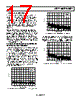
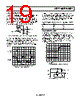
18 / 24 page  AD8571/AD8572/AD8574 Rev. C | Page 18 of 24 BROADBAND AND EXTERNAL RESISTOR NOISE CONSIDERATIONS The total broadband noise output from any amplifier is primarily a function of three types of noise: input voltage noise from the amplifier, input current noise from the amplifier, and Johnson noise from the external resistors used around the amplifier. Input voltage noise, or en, is strictly a function of the amplifier used. The Johnson noise from a resistor is a function of the resistance and the temperature. Input current noise, or in, creates an equivalent voltage noise proportional to the resistors used around the amplifier. These noise sources are not correlated with each other and their combined noise sums in a root- squared-sum fashion. The full equation is given as 2 / 1 2 2 , ] ) ( 4 [ s n s n TOTAL n r i kTr e e + + = (15) The output overdrive recovery for an autocorrection amplifier is defined as the time it takes for the output to correct to its final voltage from an overload state. It is measured by placing the amplifier in a high gain configuration with an input signal that forces the output voltage to the supply rail. The input voltage is then stepped down to the linear region of the amplifier, usually to halfway between the supplies. The time from the input signal step-down to the output settling to within 100 μV of its final value is the overdrive recovery time. Many autocorrection amplifiers require a number of auto-zero clock cycles to recover from output overdrive, and some can take several milliseconds for the output to settle properly. INPUT OVERVOLTAGE PROTECTION where: e Although the AD857x are rail-to-rail input amplifiers, care should be taken to ensure that the potential difference between the inputs does not exceed 5 V. Under normal operating conditions, the amplifier corrects its output to ensure the two inputs are at the same voltage. However, if the device is configured as a comparator, or is under some unusual operating condition, the input voltages may be forced to different potentials, which could cause excessive current to flow through the internal diodes in the AD857x used to protect the input stage against overvoltage. n is the input voltage noise of the amplifier. in is the input current noise of the amplifier. rs is the source resistance connected to the noninverting terminal. k is Boltzmann’s constant (1.38 × 10⁻²³ J/K). T is the ambient temperature in Kelvin (K = 273.15 + °C). The input voltage noise density, en, of the AD857x is 51 nV/√Hz, and the input noise, in, is 2 fA/√Hz. The en, TOTAL is dominated by the input voltage noise provided that the source resistance is less than 172 kΩ. With source resistance greater than 172 kΩ, the overall noise of the system is dominated by the Johnson noise of the resistor itself. If either input exceeds either supply rail by more than 0.3 V, large amounts of current begin to flow through the ESD protection diodes in the amplifier. These diodes are connected between the inputs and each supply rail to protect the input transistors against an electrostatic discharge event and are normally reverse-biased. However, if the input voltage exceeds the supply voltage, these ESD diodes become forward-biased. Without current-limiting, excessive amounts of current can flow through these diodes, causing permanent damage to the device. If inputs are subject to overvoltage, appropriate series resistors should be inserted to limit the diode current to less than 2 mA. Because the input current noise of the AD857x is very small, in does not become a dominant term unless rs > 4 GΩ, which is an impractical value of source resistance. The total noise, en, TOTAL, is expressed in volts-per-square-root Hertz, and the equivalent rms noise over a certain bandwidth can be found as BW e e TOTAL n n × = , (16) OUTPUT PHASE REVERSAL where BW is the bandwidth of interest in Hertz. Output phase reversal occurs in some amplifiers when the input common-mode voltage range is exceeded. As common-mode voltage moves outside the common-mode range, the outputs of these amplifiers suddenly jump in the opposite direction to the supply rail. This is the result of the differential input pair shutting down, causing a radical shifting of internal voltages that results in the erratic output behavior. OUTPUT OVERDRIVE RECOVERY The AD857x amplifiers have an excellent overdrive recovery of only 200 μs from either supply rail. This characteristic is particularly difficult for autocorrection amplifiers because the nulling amplifier requires a substantial amount of time to error correct the main amplifier back to a valid output. Figure 29 and Figure 30 show the positive and negative overdrive recovery times for the AD857x. The AD857x amplifier has been carefully designed to prevent any output phase reversal, provided both inputs are maintained within the supply voltages. If one or both inputs exceed either supply voltage, a resistor should be placed in series with the input to limit the current to less than 2 mA to ensure the output does not reverse its phase. |
|
|
链接网址 |
| ALLDATASHEET是否为您带来帮助? [ DONATE ] |
关于 Alldatasheet | 广告服务 | 联系我们 | 隐私政策 | 数据表链接 | 链接交换 | 制造商名单 All Rights Reserved©Alldatasheet.com |
| Russian : Alldatasheetru.com | Korean : Alldatasheet.co.kr | Spanish : Alldatasheet.es | French : Alldatasheet.fr | Italian : Alldatasheetit.com Portuguese : Alldatasheetpt.com | Polish : Alldatasheet.pl | Vietnamese : Alldatasheet.vn Indian : Alldatasheet.in | Mexican : Alldatasheet.com.mx | British : Alldatasheet.co.uk | New Zealand : Alldatasheet.co.nz |
|
Family Site : ic2ic.com |
icmetro.com |
 Chinese ▼
 English
 Chinese
 German
 Japanese
 Russian
 Korean
 Spanish
 French
 Italian
 Portuguese
 Polish
 Vietnamese
 Indian
 Mexican
 British
 New Zealand