|
数据搜索系统,热门电子元器件搜索 |
|
|
数据搜索系统,热门电子元器件搜索 |
|
AD8571ARMZ-R2 数据表(PDF) 16 Page - Analog Devices |
|
|
|||||||||||||||||||||||||||||
AD8571ARMZ-R2 数据表(HTML) 16 Page - Analog Devices |
|
|
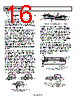
16 / 24 page  AD8571/AD8572/AD8574 Rev. C | Page 16 of 24 Therefore, A OSB OSA EFF OS B V V V + ≈ , (14) V– V+ VREF VREF VIN1 VIN2 GUARD RING R1 R2 R2 R1 AD8572 GUARD RING Thus, the offset voltages of both the primary and nulling amplifiers are reduced by the gain factor BA, which takes a typical input offset voltage from several millivolts down to an effective input offset voltage of submicrovolts. This autocorrection scheme makes the AD857x family of amplifiers extremely precise. Figure 53. Top View of AD8572 SOIC Layout with Guard Rings Other potential sources of offset error are thermoelectric voltages on the circuit board. This voltage, also called Seebeck voltage, occurs at the junction of two dissimilar metals and is proportional to the junction temperature. The most common metallic junctions on a circuit board are solder-to-board trace and solder-to-component lead. HIGH GAIN, CMRR, AND PSRR Common-mode and power supply rejection are indications of the amount of offset voltage an amplifier has as a result of a change in its input common-mode or power supply voltages. As shown in the Figure 54 shows a cross-section view of the thermal voltage error sources. When the temperature of the PCB at one end of the component (T Amplification Phase section, the autocorrection architecture of the AD857x allows it to effectively minimize offset voltages. The technique also corrects for offset errors caused by common-mode voltage swings and power supply variations, which results in superb CMRR and PSRR figures in excess of 130 dB. Because the autocorrection occurs continuously, these figures can be maintained across the entire temperature range of the device, from −40°C to +125°C. A1 ) differs from the temperature at the other end (TA2), the Seebeck voltages are not equal, resulting in a thermal voltage error. This thermocouple error can be reduced by using dummy components to match the thermoelectric error source. Placing the dummy component as close as possible to its partner ensures both Seebeck voltages are equal, thus canceling the thermocouple error. Maintaining a constant ambient temperature on the circuit board further reduces this error. The use of a ground plane helps distribute heat throughout the board and also reduces EMI noise pickup. MAXIMIZING PERFORMANCE THROUGH PROPER LAYOUT To achieve the maximum performance of the extremely high input impedance and low offset voltage of the AD857x, care should be taken in the circuit board layout. The PCB surface must remain clean and free of moisture to avoid leakage currents between adjacent traces. Surface coating of the circuit board reduces surface moisture and provides a humidity barrier, reducing parasitic resistance on the board. The use of guard rings around the amplifier inputs further reduces leakage currents. SURFACE MOUNT COMPONENT COMPONENT LEAD SOLDER PC BOARD COPPER TRACE TA2 IF TA1 ≠ TA2, THEN VTS1 + VSC1 ≠ VTS2 + VSC2 TA1 VSC1 VTS1 + – + – VSC2 VTS2 + + – – Figure 52 shows how the guard ring should be configured, and Figure 53 shows the top view of how a surface-mount layout can be arranged. The guard ring does not need to be a specific width, but it should form a continuous loop around both inputs. By setting the guard ring voltage equal to the voltage at the noninverting input, parasitic capacitance is minimized as well. For further reduction of leakage currents, components can be mounted to the PCB using Teflon® standoff insulators. Figure 54. Mismatch in Seebeck Voltages Causes a Thermoelectric Voltage Error RS SHOULD BE PLACED IN CLOSE PROXIMITY AND ALIGNMENT TO R1 TO BALANCE SEEBECK VOLTAGES VOUT VIN AD8571/AD8572/ AD8574 AV = 1 + (RF /R1) RF RS = R1 R1 VOUT VOUT VOUT VIN AD8572 VIN AD8572 V IN AD8572 Figure 55. Using Dummy Components to Cancel Thermoelectric Voltage Errors Figure 52. Guard Ring Layout and Connections to Reduce PCB Leakage Currents |
|
|
链接网址 |
| ALLDATASHEET是否为您带来帮助? [ DONATE ] |
关于 Alldatasheet | 广告服务 | 联系我们 | 隐私政策 | 数据表链接 | 链接交换 | 制造商名单 All Rights Reserved©Alldatasheet.com |
| Russian : Alldatasheetru.com | Korean : Alldatasheet.co.kr | Spanish : Alldatasheet.es | French : Alldatasheet.fr | Italian : Alldatasheetit.com Portuguese : Alldatasheetpt.com | Polish : Alldatasheet.pl | Vietnamese : Alldatasheet.vn Indian : Alldatasheet.in | Mexican : Alldatasheet.com.mx | British : Alldatasheet.co.uk | New Zealand : Alldatasheet.co.nz |
|
Family Site : ic2ic.com |
icmetro.com |
 Chinese ▼
 English
 Chinese
 German
 Japanese
 Russian
 Korean
 Spanish
 French
 Italian
 Portuguese
 Polish
 Vietnamese
 Indian
 Mexican
 British
 New Zealand