|
数据搜索系统,热门电子元器件搜索 |
|
|
数据搜索系统,热门电子元器件搜索 |
|
AD8606ARM-R2 数据表(PDF) 16 Page - Analog Devices |
|
|
|||||||||||||||||||||||||||||
AD8606ARM-R2 数据表(HTML) 16 Page - Analog Devices |
|
|
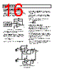
16 / 20 page  AD8605/AD8606/AD8608 Rev. D | Page 16 of 20 I-V CONVERSION APPLICATIONS PHOTODIODE PREAMPLIFIER APPLICATIONS The low offset voltage and input current of the AD8605 make it an excellent choice for photodiode applications. In addition, the low voltage and current noise make the amplifier ideal for application circuits with high sensitivity. RD ID CD 50pF AD8605 VOUT PHOTODIODE +VOS– RF 10M Ω CF 10pF Figure 51. Equivalent Circuit for Photodiode Preamp The input bias current of the amplifier contributes an error term that is proportional to the value of RF. The offset voltage causes a dark current induced by the shunt resistance of the diode RD. These error terms are combined at the output of the amplifier. The error voltage is written as B F D F OS O I R R R V E + ⎟⎟ ⎠ ⎞ ⎜⎜ ⎝ ⎛ + = 1 Typically, RF is smaller than RD, thus RF/RD can be ignored. At room temperature, the AD8605 has an input bias current of 0.2 pA and an offset voltage of 100 µV. Typical values of RD are in the range of 1 GΩ. For the circuit shown in Figure 9, the output error voltage is approximately 100 µV at room temperature, increasing to about 1 mV at 85°C. Where ft is the unity gain frequency of the amplifier, the maximum achievable signal bandwidth is T F t MAX C R f f π = 2 AUDIO AND PDA APPLICATIONS The AD8605’s low distortion and wide dynamic range make it a great choice for audio and PDA applications, including microphone amplification and line output buffering. Figure 52 shows a typical application circuit for headphone/line out amplification. R1 and R2 are used to bias the input voltage at half the supply. This maximizes the signal bandwidth range. C1 and C2 are used to ac couple the input signal. C1 and R2 form a high-pass filter whose corner frequency is 1/2πR1C1. The high output current of the AD8605 allows it to drive heavy resistive loads. The circuit of Figure 52 was tested to drive a 16 W headphone. The THD + N is maintained at approximately −60 dB throughout the audio range. 5V 4 2 3 8 1 HEADPHONES 5V 4 6 5 8 7 C1 1 µF R1 10k Ω R2 10k Ω V1 500mV 1/2 AD8606 C3 100 µF R4 20 Ω R3 1k Ω 1/2 AD8606 C4 100 µF R6 20 Ω R5 1k Ω C2 1 µF V2 500mV Figure 52. Single-Supply Headphone/Speaker Amplifier |
|
|
链接网址 |
| ALLDATASHEET是否为您带来帮助? [ DONATE ] |
关于 Alldatasheet | 广告服务 | 联系我们 | 隐私政策 | 数据表链接 | 链接交换 | 制造商名单 All Rights Reserved©Alldatasheet.com |
| Russian : Alldatasheetru.com | Korean : Alldatasheet.co.kr | Spanish : Alldatasheet.es | French : Alldatasheet.fr | Italian : Alldatasheetit.com Portuguese : Alldatasheetpt.com | Polish : Alldatasheet.pl | Vietnamese : Alldatasheet.vn Indian : Alldatasheet.in | Mexican : Alldatasheet.com.mx | British : Alldatasheet.co.uk | New Zealand : Alldatasheet.co.nz |
|
Family Site : ic2ic.com |
icmetro.com |
 Chinese ▼
 English
 Chinese
 German
 Japanese
 Russian
 Korean
 Spanish
 French
 Italian
 Portuguese
 Polish
 Vietnamese
 Indian
 Mexican
 British
 New Zealand