|
数据搜索系统,热门电子元器件搜索 |
|
|
数据搜索系统,热门电子元器件搜索 |
|
ADP191ACBZ-R7 数据表(PDF) 10 Page - Analog Devices |
|
|
|||||||||||||||||||||||||||||
ADP191ACBZ-R7 数据表(HTML) 10 Page - Analog Devices |
|
|
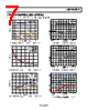
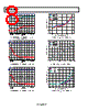
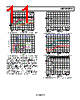
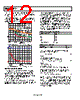
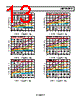
10 / 16 page  ADP190/ADP191 Rev. D | Page 10 of 16 APPLICATIONS INFORMATION GROUND CURRENT The major source for ground current in the ADP190/ADP191 is the 4 MΩ pull-down on the enable (EN) pin. Figure 19 shows typical ground current when VEN = VIN and VIN varies from 1.1 V to 3.6 V. 2.0 1.8 1.6 1.4 1.2 1.0 0.6 0.8 350 300 250 200 150 100 50 0 LOAD (mA) VIN = 1.2V VIN = 1.8V VIN = 2.5V VIN = 3.6V Figure 19. Ground Current vs. Load Current As shown in Figure 20, an increase in ground current can occur when VEN ≠ VIN. This is caused by the CMOS logic nature of the level shift circuitry as it translates an EN signal ≥ 1.1 V to a logic high. This increase is a function of the VIN − VEN delta. 14 12 10 8 6 4 2 0 3.5 0.1 0.3 0.5 0.7 0.9 1.1 1.3 1.5 1.7 1.9 2.1 2.3 2.5 2.7 3.3 3.1 2.9 VEN (V) VOUT = 1.8V VOUT = 3.6V Figure 20. Typical Ground Current when VEN ≠ VIN ENABLE FEATURE The ADP190/ADP191 use the EN pin to enable and disable the VOUT pin under normal operating conditions. As shown in Figure 21, when a rising voltage on EN crosses the active threshold, VOUT turns on. When a falling voltage on EN crosses the inactive threshold, VOUT turns off. 2.0 1.8 1.6 1.4 1.2 1.0 0.8 0.6 0.4 0.2 0 1.2 00.4 0.5 0.6 0.7 0.1 0.2 0.3 0.8 0.9 1.0 1.1 VEN (V) Figure 21. Typical EN Operation As shown in Figure 21, the EN pin has built-in hysteresis. This prevents on/off oscillations that can occur due to noise on the EN pin as it passes through the threshold points. The EN pin active/inactive thresholds derive from the VIN voltage; therefore, these thresholds vary with changing input voltage. Figure 22 shows typical EN active/inactive thresholds when the input voltage varies from 1.1 V to 3.6 V. 1.15 1.05 0.95 0.85 0.75 0.65 0.55 0.45 0.35 VIN (V) EN ACTIVE EN INACTIVE Figure 22. Typical EN Pin Thresholds vs. Input Voltage, VIN TIMING Turn-on delay is defined as the delta between the time that EN reaches >1.1 V until VOUT rises to ~10% of its final value. The ADP190/ADP191 include circuitry to set the typical 1.5 μs turn- on delay at 3.6 V VIN to limit the VIN inrush current. As shown in Figure 23, the turn-on delay is dependent on the input voltage. |
|
|
链接网址 |
| ALLDATASHEET是否为您带来帮助? [ DONATE ] |
关于 Alldatasheet | 广告服务 | 联系我们 | 隐私政策 | 数据表链接 | 链接交换 | 制造商名单 All Rights Reserved©Alldatasheet.com |
| Russian : Alldatasheetru.com | Korean : Alldatasheet.co.kr | Spanish : Alldatasheet.es | French : Alldatasheet.fr | Italian : Alldatasheetit.com Portuguese : Alldatasheetpt.com | Polish : Alldatasheet.pl | Vietnamese : Alldatasheet.vn Indian : Alldatasheet.in | Mexican : Alldatasheet.com.mx | British : Alldatasheet.co.uk | New Zealand : Alldatasheet.co.nz |
|
Family Site : ic2ic.com |
icmetro.com |
 Chinese ▼
 English
 Chinese
 German
 Japanese
 Russian
 Korean
 Spanish
 French
 Italian
 Portuguese
 Polish
 Vietnamese
 Indian
 Mexican
 British
 New Zealand