|
数据搜索系统,热门电子元器件搜索 |
|
|
数据搜索系统,热门电子元器件搜索 |
|
ADP191ACBZ-R7 数据表(PDF) 11 Page - Analog Devices |
|
|
|||||||||||||||||||||||||||||
ADP191ACBZ-R7 数据表(HTML) 11 Page - Analog Devices |
|
|
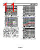
11 / 16 page  ADP190/ADP191 Rev. D | Page 11 of 16 2 CH1 1V CH2 1V M4µs A CH1 2.34V T 15.96µs 1 T ILOAD = 100mA CLOAD = 1µF VEN = 3.6V VOUT = 1.2V VOUT = 1.8V VOUT = 2.5V VEN Figure 23. ADP190 Typical Turn-On Delay Time with Varying Input Voltage 4.0 3.5 3.0 2.5 2.0 1.5 1.0 0.5 0 500 0 100 200 300 400 TIME (µs) VEN = 1.8V VOUT = 1.2V VOUT = 1.8V VOUT = 3.6V Figure 24. ADP191 Typical Turn-On Delay Time with Varying Input Voltage The rise time is defined as the delta between the time from 10% to 90% of VOUT reaching its final value. It is dependent on the RC time constant where C = load capacitance (CLOAD) and R = RDSON||RLOAD. Because RDSON is usually smaller than RLOAD, an adequate approximation for RC is RDSON × CLOAD. The ADP190/ ADP191 do not need any input or load capacitor, but capacitors can be used to suppress noise on the board. If significant load capacitance is connected, inrush current is a concern. The ADP191 contains circuitry to limit the slew rate of the switch turn to reduce the turn on inrush current. See Figure 25 and Figure 26 for a comparison of rise time and inrush current. 2 3 CH1 2V CH3 2.00mA Ω CH2 2V M10µs A CH1 2.32V T 40.16µs 1 T VOUT = 1.8V ILOAD = 200mA CLOAD = 1µF VEN = 3.6V VEN VOUT IIN Figure 25. ADP190 Typical Rise Time and Inrush Current with CLOAD = 1 μF 2 3 CH1 2.00V CH2 100mA CH3 2.00V M20.0µs A CH1 1.24V T 10.20% 1 VEN IIN VOUT T Figure 26. ADP191 Typical Rise Time and Inrush Current with CLOAD = 1 μF 2 3 CH1 2V CH3 2.00mA Ω CH2 2V M10µs A CH1 1.00V T 39.8µs 1 VOUT = 1.8V ILOAD = 200mA CLOAD = 4.7µF VEN= 3.6V VEN VOUT IIN T Figure 27. ADP190 Typical Rise Time and Inrush Current with CLOAD = 4.7 μF |
|
|
链接网址 |
| ALLDATASHEET是否为您带来帮助? [ DONATE ] |
关于 Alldatasheet | 广告服务 | 联系我们 | 隐私政策 | 数据表链接 | 链接交换 | 制造商名单 All Rights Reserved©Alldatasheet.com |
| Russian : Alldatasheetru.com | Korean : Alldatasheet.co.kr | Spanish : Alldatasheet.es | French : Alldatasheet.fr | Italian : Alldatasheetit.com Portuguese : Alldatasheetpt.com | Polish : Alldatasheet.pl | Vietnamese : Alldatasheet.vn Indian : Alldatasheet.in | Mexican : Alldatasheet.com.mx | British : Alldatasheet.co.uk | New Zealand : Alldatasheet.co.nz |
|
Family Site : ic2ic.com |
icmetro.com |
 Chinese ▼
 English
 Chinese
 German
 Japanese
 Russian
 Korean
 Spanish
 French
 Italian
 Portuguese
 Polish
 Vietnamese
 Indian
 Mexican
 British
 New Zealand