|
数据搜索系统,热门电子元器件搜索 |
|
|
数据搜索系统,热门电子元器件搜索 |
|
ADR03BKS-R2 数据表(PDF) 15 Page - Analog Devices |
|
|
|||||||||||||||||||||||||||||
ADR03BKS-R2 数据表(HTML) 15 Page - Analog Devices |
|
|
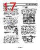
15 / 20 page  Data Sheet ADR01/ADR02/ADR03/ADR06 Rev. R | Page 15 of 20 APPLICATIONS INFORMATION OVERVIEW The ADR01/ADR02/ADR03/ADR06 are high precision, low drift 10.0 V, 5.0 V, 2.5 V, and 3.0 V voltage references available in an ultracompact footprint. The 8-lead SOIC versions of the devices are drop-in replacements of the REF01/REF02/REF03 sockets with improved cost and performance. These devices are standard band gap references (see Figure 34). The band gap cell contains two NPN transistors (Q18 and Q19) that differ in emitter area by 2×. The difference in their VBE produces a proportional-to-absolute temperature current (PTAT) in R14, and, when combined with the VBE of Q19, produces a band gap voltage, VBG, that is almost constant in temperature. With an internal op amp and the feedback network of R5 and R6, VO is set precisely at 10.0 V, 5.0 V, 2.5 V, and 3.0 V for the ADR01, ADR02, ADR06, and ADR03, respectively. Precision laser trimming of the resistors and other proprietary circuit techniques are used to further enhance the initial accuracy, temperature curvature, and drift performance of the ADR01/ ADR02/ADR03/ADR06. The PTAT voltage is made available at the TEMP pin of the ADR01/ADR02/ADR03/ADR06. It has a stable 1.96 mV/°C temperature coefficient, such that users can estimate the temperature change of the device by knowing the voltage change at the TEMP pin. APPLYING THE ADR01/ADR02/ADR03/ADR06 Input and Output Capacitors Although the ADR01/ADR02/ADR03/ADR06 are designed to function stably without any external components, connecting a 0.1 μF ceramic capacitor to the output is highly recommended to improve stability and filter out low level voltage noise. An additional 1 μF to 10 μF electrolytic, tantalum, or ceramic capacitor can be added in parallel to improve transient per- formance in response to sudden changes in load current; however, the designer should keep in mind that doing so increases the turn-on time of the device. A 1 μF to 10 μF electrolytic, tantalum or ceramic capacitor can also be connected to the input to improve transient response in applications where the supply voltage may fluctuate. An addi- tional 0.1 μF ceramic capacitor should be connected in parallel to reduce supply noise. Mount both input and output capacitors as close to the device pins as possible. Output Adjustment The ADR01/ADR02/ADR03/ADR06 trim terminal can be used to adjust the output voltage over a nominal voltage. This feature allows a system designer to trim system errors by setting the reference to a voltage other than 10.0 V/5.0 V/2.5 V/3.0 V. For finer adjustment, add a series resistor of 470 kΩ. With the con- figuration shown in Figure 35, the ADR01 can be adjusted from 9.70 V to 10.05 V, the ADR02 can be adjusted from 4.95 V to 5.02 V, the ADR06 can be adjusted from 2.8 V to 3.3 V, and the ADR03 can be adjusted from 2.3 V to 2.8 V. Adjustment of the output does not significantly affect the temperature performance of the device, provided the temperature coefficients of the resis- tors are relatively low. U1 ADR01/ ADR02/ ADR03/ ADR06 VO C2 0.1µF C1 0.1µF VIN VIN VOUT TEMP TRIM GND Figure 33. Basic Configuration R1 R2 R3 R4 VIN Q23 Q1 Q2 Q7 Q8 Q9 Q3 Q10 D1 D2 Q4 VO D3 C1 R13 Q12 Q13 R5 I1 R12 Q14 Q15 2× 1× VBG R20 TRIM Q18 TEMP R27 Q19 Q16 Q17 Q20 R6 R42 R41 R24 R32 R11 R17 R14 GND Figure 34. Simplified Schematic Diagram U1 ADR01/ ADR02/ ADR03/ ADR06 VIN VOUT TEMP TRIM GND VIN VO POT 10kΩ R2 1kΩ R1 470kΩ Figure 35. Optional Trim Adjustment Temperature Monitoring As described at the end of the Overview section, the ADR01/ ADR02/ADR03/ADR06 provide a TEMP output (Pin 1 in Figure 1 and Pin 3 in Figure 2) that varies linearly with temperature. This output can be used to monitor the temperature change in the system. The voltage at VTEMP is approximately 550 mV at 25°C, and the temperature coefficient is approximately 1.96 mV/°C (see Figure 36). A voltage change of 39.2 mV at the TEMP pin corresponds to a 20°C change in temperature. |
|
|
链接网址 |
| ALLDATASHEET是否为您带来帮助? [ DONATE ] |
关于 Alldatasheet | 广告服务 | 联系我们 | 隐私政策 | 数据表链接 | 链接交换 | 制造商名单 All Rights Reserved©Alldatasheet.com |
| Russian : Alldatasheetru.com | Korean : Alldatasheet.co.kr | Spanish : Alldatasheet.es | French : Alldatasheet.fr | Italian : Alldatasheetit.com Portuguese : Alldatasheetpt.com | Polish : Alldatasheet.pl | Vietnamese : Alldatasheet.vn Indian : Alldatasheet.in | Mexican : Alldatasheet.com.mx | British : Alldatasheet.co.uk | New Zealand : Alldatasheet.co.nz |
|
Family Site : ic2ic.com |
icmetro.com |
 Chinese ▼
 English
 Chinese
 German
 Japanese
 Russian
 Korean
 Spanish
 French
 Italian
 Portuguese
 Polish
 Vietnamese
 Indian
 Mexican
 British
 New Zealand