|
数据搜索系统,热门电子元器件搜索 |
|
|
数据搜索系统,热门电子元器件搜索 |
|
ADR03BKS-R2 数据表(PDF) 16 Page - Analog Devices |
|
|
|||||||||||||||||||||||||||||
ADR03BKS-R2 数据表(HTML) 16 Page - Analog Devices |
|
|
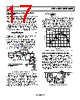
16 / 20 page  ADR01/ADR02/ADR03/ADR06 Data Sheet Rev. R | Page 16 of 20 125 25 50 75 100 0.40 0.80 0.75 0.70 0.65 0.60 0.55 0.50 0.45 –25 0 –50 VIN = 15V SAMPLE SIZE = 5 TEMPERATURE (°C) ΔV TEMP /ΔT ≈ 1.96mV/°C Figure 36. Voltage at TEMP Pin vs. Temperature The TEMP function is provided as a convenience rather than a precise feature. Because the voltage at the TEMP node is acquired from the band gap core, current pulling from this pin has a significant effect on VOUT. Care must be taken to buffer the TEMP output with a suitable low bias current op amp, such as the AD8601, AD820, or OP1177, all of which result in less than a 100 µV change in ∆VOUT (see Figure 37). Without buffering, even tens of microamps drawn from the TEMP pin can cause VOUT to fall out of specification. U2 15V U1 ADR01/ ADR02/ ADR03/ ADR06 VIN VOUT TEMP TRIM GND VO V– V+ OP1177 VTEMP 1.9mV/°C VIN Figure 37. Temperature Monitoring LOW COST CURRENT SOURCE Unlike most references, the ADR01/ADR02/ADR03/ADR06 employ an NPN Darlington in which the quiescent current remains constant with respect to the load current, as shown in Figure 23. As a result, a current source can be configured as shown in Figure 38 where ISET = (VOUT − VL)/RSET. IL is simply the sum of ISET and IQ. Although simple, IQ varies typically from 0.55 mA to 0.65 mA, limiting this circuit to general-purpose applications. ADR01/ ADR02/ ADR03/ ADR06 VOUT GND VIN IIN ISET = (VOUT – VL)/RSET RSET IQ ≈ 0.6mA IL = ISET + IQ VL RL Figure 38. Low Cost Current Source PRECISION CURRENT SOURCE WITH ADJUSTABLE OUTPUT Alternatively, a precision current source can be implemented with the circuit shown in Figure 39. By adding a mechanical or digital potentiometer, this circuit becomes an adjustable current source. If a digital potentiometer is used, the load current is simply the voltage across Terminal B to Terminal W of the digital potentiometer divided by RSET. SET REF L R D V I × = (1) where D is the decimal equivalent of the digital potentiometer input code. U2 +12V –12V W B A U1 ADR01/ ADR02/ ADR03/ ADR06 VIN VOUT TEMP TRIM GND V– V+ OP1177 –5V TO VL AD5201 0V TO (5V + VL) +12V RSET 1kΩ RL IL VL 1kΩ 100k Ω Figure 39. Programmable 0 mA to 5 mA Current Source To optimize the resolution of this circuit, dual-supply op amps should be used because the ground potential of ADR02 can swing from −5.0 V at zero scale to VL at full scale of the potentiometer setting. |
|
|
链接网址 |
| ALLDATASHEET是否为您带来帮助? [ DONATE ] |
关于 Alldatasheet | 广告服务 | 联系我们 | 隐私政策 | 数据表链接 | 链接交换 | 制造商名单 All Rights Reserved©Alldatasheet.com |
| Russian : Alldatasheetru.com | Korean : Alldatasheet.co.kr | Spanish : Alldatasheet.es | French : Alldatasheet.fr | Italian : Alldatasheetit.com Portuguese : Alldatasheetpt.com | Polish : Alldatasheet.pl | Vietnamese : Alldatasheet.vn Indian : Alldatasheet.in | Mexican : Alldatasheet.com.mx | British : Alldatasheet.co.uk | New Zealand : Alldatasheet.co.nz |
|
Family Site : ic2ic.com |
icmetro.com |
 Chinese ▼
 English
 Chinese
 German
 Japanese
 Russian
 Korean
 Spanish
 French
 Italian
 Portuguese
 Polish
 Vietnamese
 Indian
 Mexican
 British
 New Zealand