|
数据搜索系统,热门电子元器件搜索 |
|
|
数据搜索系统,热门电子元器件搜索 |
|
ADR03BKS-R2 数据表(PDF) 17 Page - Analog Devices |
|
|
|||||||||||||||||||||||||||||
ADR03BKS-R2 数据表(HTML) 17 Page - Analog Devices |
|
|
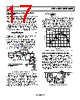
17 / 20 page  Data Sheet ADR01/ADR02/ADR03/ADR06 Rev. R | Page 17 of 20 PROGRAMMABLE 4 mA TO 20 mA CURRENT TRANSMITTER Because of their precision, adequate current handling, and small footprint, the devices are suitable as the reference sources for many high performance converter circuits. One of these applications is the multichannel 16-bit, 4 mA to 20 mA current transmitter in the industrial control market (see Figure 40). This circuit employs a Howland current pump at the output to yield better efficiency, a lower component count, and a higher voltage compliance than the conventional design with op amps and MOSFETs. In this circuit, if the resistors are matched such that R1 = R1′, R2 = R2′, R3 = R3′, the load current is N REF L D V R3 R1 R3) (R2 I 2 × × ′ + = (2) where D is similarly the decimal equivalent of the DAC input code and N is the number of bits of the DAC. According to Equation 2, R3′ can be used to set the sensitivity. R3′ can be made as small as necessary to achieve the current needed within U4 output current driving capability. Alter- natively, other resistors can be kept high to conserve power. In this circuit, the AD8512 is capable of delivering 20 mA of current, and the voltage compliance approaches 15.0 V. U1 15V VIN VOUT GND TEMP TRIM U1 = ADR01/ADR02/ADR03/ADR06, REF01 U2 = AD5543/AD5544/AD5554 U3, U4 = AD8512 U2 5V 10V +15V –15V VDD VREF GND RF IO IO AD5544 DIGITAL INPUT CODE 20%–100% FUL L SCALE U3 VX 0V TO –10V R1 150kΩ R2 15kΩ U4 C1 10pF VP R3 50Ω AD8512 R3' 50Ω VL R1' 150kΩ LOAD 500Ω 4mA TO 20mA VN VO R2' 15kΩ Figure 40. Programmable 4 mA to 20 mA Transmitter The Howland current pump yields a potentially infinite output impedance, that is highly desirable, but resistance matching is critical in this application. The output impedance can be deter- mined using Equation 3. As shown by this equation, if the resistors are perfectly matched, ZO is infinite. Alternatively, if they are not matched, ZO is either positive or negative. If the latter is true, oscillation can occur. For this reason, connect Capacitor C1 in the range of 1 pF to 10 pF between VP and the output terminal of U4 to filter any oscillation. − ′ ′ ′ = = 1 R1R2 R2 R1 R1 I V Z t t O (3) In this circuit, an ADR01 provides the stable 10.000 V reference for the AD5544 quad 16-bit DAC. The resolution of the adjust- able current is 0.3 µA/step; the total worst-case INL error is merely 4 LSBs. Such error is equivalent to 1.2 µA or a 0.006% system error, which is well below most systems’ requirements. The result is shown in Figure 41 with measurement taken at 25°C and 70°C; total system error of 4 LSBs at both 25°C and 70°C. 5 –1 0 65536 8192 16384 24576 32768 40960 49152 57344 4 3 2 1 0 CODE (Decimal) RL = 500Ω IL = 0mA TO 20mA 25°C 70°C Figure 41. Result of Programmable 4 mA to 20 mA Current Transmitter PRECISION BOOSTED OUTPUT REGULATOR A precision voltage output with boosted current capability can be realized with the circuit shown in Figure 42. In this circuit, U2 forces VO to be equal to VREF by regulating the turn-on of N1, thereby making the load current furnished by VIN. In this configuration, a 50 mA load is achievable at VIN of 15.0 V. Moderate heat is generated on the MOSFET, and higher current can be achieved with a replacement of a larger device. In addition, for a heavy capacitive load with a fast edging input signal, a buffer should be added at the output to enhance the transient response. U2 15V N1 200Ω U1 ADR01/ ADR02/ ADR03/ ADR06 VIN VOUT TEMP TRIM GND V– V+ OP1177 2N7002 VIN VO RL 1µF CL C1 1000pF R2 100Ω R1 100Ω Figure 42. Precision Boosted Output Regulator |
|
|
链接网址 |
| ALLDATASHEET是否为您带来帮助? [ DONATE ] |
关于 Alldatasheet | 广告服务 | 联系我们 | 隐私政策 | 数据表链接 | 链接交换 | 制造商名单 All Rights Reserved©Alldatasheet.com |
| Russian : Alldatasheetru.com | Korean : Alldatasheet.co.kr | Spanish : Alldatasheet.es | French : Alldatasheet.fr | Italian : Alldatasheetit.com Portuguese : Alldatasheetpt.com | Polish : Alldatasheet.pl | Vietnamese : Alldatasheet.vn Indian : Alldatasheet.in | Mexican : Alldatasheet.com.mx | British : Alldatasheet.co.uk | New Zealand : Alldatasheet.co.nz |
|
Family Site : ic2ic.com |
icmetro.com |
 Chinese ▼
 English
 Chinese
 German
 Japanese
 Russian
 Korean
 Spanish
 French
 Italian
 Portuguese
 Polish
 Vietnamese
 Indian
 Mexican
 British
 New Zealand