|
数据搜索系统,热门电子元器件搜索 |
|
|
数据搜索系统,热门电子元器件搜索 |
|
LTC1663CMS8 数据表(PDF) 7 Page - Linear Technology |
|
|
|||||||||||||||||||||||||||||
LTC1663CMS8 数据表(HTML) 7 Page - Linear Technology |
|
|
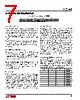
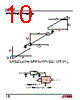
7 / 12 page  7 LTC1663 Serial Digital Interface The LTC1663 communicates with a host (master) using the standard 2-wire interface. The Timing Diagram shows the timing relationship of the signals on the bus. The two bus lines, SDA and SCL, must be high when the bus is not in use. External pull-up resistors or current sources, such as the LTC1694 SMBus Accelerator, are required on these lines. The LTC1663 is a receive-only (slave) device. The master can communicate with the LTC1663 using the Quick Command, Send Byte or Write Word protocols as ex- plained later. The START and STOP Conditions When the bus is not in use, both SCL and SDA must be high. A bus master signals the beginning of a communica- tion to a slave device by transmitting a START condition. A START condition is generated by transitioning SDA from high to low while SCL is high. When the master has finished communicating with the slave, it issues a STOP condition. A STOP condition is generated by transitioning SDA from low to high while SCL is high. The bus is then free for communication with another SMBus device. Acknowledge The Acknowledge signal is used for handshaking between the master and the slave. An Acknowledge (active LOW) generated by the slave lets the master know that the latest byte of information was received. The Acknowledge re- lated clock pulse is generated by the master. The master releases the SDA line (HIGH) during the Acknowledge clock pulse. The slave-receiver must pull down the SDA line during the Acknowledge clock pulse so that it remains a stable LOW during the HIGH period of this clock pulse. Write Word Protocol The master initiates communication with the LTC1663 with a START condition and a 7-bit address followed by the Write Bit (Wr) = 0. The LTC1663 acknowledges and the master delivers the command byte. The LTC1663 ac- knowledges and latches the command byte into the com- mand byte input register. The master then delivers the least significant data byte. Again the LTC1663 acknowl- edges and the data is latched into the least significant data byte input register. The master then delivers the most significant data byte. The LTC1663 acknowledges once more and latches the data into the most significant data byte input register. Lastly, the master terminates the communication with a STOP condition. On the reception of the STOP condition, the LTC1663 transfers the input register information to output registers and the DAC output is updated. Slave Address (MSOP Package Only) The LTC1663 can respond to one of eight 7-bit addresses. The first 4 bits (MSBs) have been factory programmed to 0100. The three address bits, AD2, AD1 and AD0 are programmed by the user and determine the LSBs of the slave address, as shown in the table below: AD2 AD1 AD0 0100 xxx L L L 0100 000 L L H 0100 001 L H L 0100 010 L H H 0100 011 H L L 0100 100 H L H 0100 101 H H L 0100 110 H H H 0100 111 APPLICATIONS INFORMATION Write Word Protocol Used by the LTC1663 Command Byte A Slave Address A Wr LSData Byte A MSData Byte A P S 81 71 18 1 8 1663 TA03 11 1 S = Start Condition, Wr = Write Bit = 0, A = Acknowledge, P = Stop Condition |
|
|
链接网址 |
| ALLDATASHEET是否为您带来帮助? [ DONATE ] |
关于 Alldatasheet | 广告服务 | 联系我们 | 隐私政策 | 数据表链接 | 链接交换 | 制造商名单 All Rights Reserved©Alldatasheet.com |
| Russian : Alldatasheetru.com | Korean : Alldatasheet.co.kr | Spanish : Alldatasheet.es | French : Alldatasheet.fr | Italian : Alldatasheetit.com Portuguese : Alldatasheetpt.com | Polish : Alldatasheet.pl | Vietnamese : Alldatasheet.vn Indian : Alldatasheet.in | Mexican : Alldatasheet.com.mx | British : Alldatasheet.co.uk | New Zealand : Alldatasheet.co.nz |
|
Family Site : ic2ic.com |
icmetro.com |
 Chinese ▼
 English
 Chinese
 German
 Japanese
 Russian
 Korean
 Spanish
 French
 Italian
 Portuguese
 Polish
 Vietnamese
 Indian
 Mexican
 British
 New Zealand