|
数据搜索系统,热门电子元器件搜索 |
|
|
数据搜索系统,热门电子元器件搜索 |
|
P9027LP-R 数据表(PDF) 10 Page - Integrated Device Technology |
|
|
|||||||||||||||||||||||||||||
P9027LP-R 数据表(HTML) 10 Page - Integrated Device Technology |
|
|
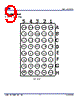
10 / 27 page  P9027LP-R Datasheet © 2016 Integrated Device Technology, Inc 10 April 28, 2016 Pin Description Table 5. Pin Description Pins Name Typical Description PGND A1, A2, A3, A4, A5, B3 GND Power ground. LX2 B1, B2 I Connect the Rx coil to this pin. LX1 B4, B5 I Connect the other side of Rx coil to this pin. RECT C1, C2, C3, C4, C5 O Output voltage of the synchronous rectifier bridge. Connect at least two 10 µF capacitors from this pin to PGND. The rectifier voltage dynamically changes as the load changes. See typical curves. CFLY2 D1 O Positive and negative terminals of the internal charge pump. Connect a 47 nF capacitor between these two pins. CFLY1 D2 O OUT D3, D4, D5 O Regulated output voltage pin. Connect at least two 10 µF capacitors from this pin to PGND. The default voltage is set to 5V when VSET is directly shorted to GND. For more information see VSET application section. NC E1, E2, E4, F2 NC Do not connect. RSVD E3 I This pin is reserved for internal use. Connect a 1.69 KΩ resistor from this pin to GND for 1 W coil. For 2 W and 3 W’s coils, use a 1.13 KΩ resistor. OUTSNS E5 I Feedback input pin. This pin must be connected directly to OUT pin to provide a regulated voltage. IOC F1 I Programmable over-current limit pin. Connect a resistor from this pin to GND to set the current-limit threshold. To disable the current-limit, connect the pin directly to GND. For more information see current limit application section. EOC F3 I Active high end of charge input pin. When connected to logic high, the device sends end of power transfer packet (charge complete) to the transmitter to terminate power transfer and shuts down. The OUT pin is high impedance after P9027LP-R is shutdown VSET F4 I Programming pin to set the output voltage. Connect a resistor from the pin to GND to set the output voltage. Shorting the pin to GND sets the output voltage to 5 V. For more information refer to the application section VSET for different output voltage settings. VHDR F5 I Programming pin to set the rectifier voltage. Connect a resistor from the pin to ground. Refer to the application section for appropriate resistor selection. VDD G1 O Charge pumps regulated 5 V supply to power the internal circuitry. Connect a 1 µF capacitor as close as possible from this pin to GND. Do not load the pin. EN G2 I Active low enable pin. Pulling this pin to logic high forces the device into shutdown mode. When connected to logic low, the device is enabled. Do not leave the pin floating. AGND G3, H1 GND Analog ground. TS2 G4 Remote temperature sensor 2. If not used, connect to AGND. |
|
|
链接网址 |
| ALLDATASHEET是否为您带来帮助? [ DONATE ] |
关于 Alldatasheet | 广告服务 | 联系我们 | 隐私政策 | 数据表链接 | 链接交换 | 制造商名单 All Rights Reserved©Alldatasheet.com |
| Russian : Alldatasheetru.com | Korean : Alldatasheet.co.kr | Spanish : Alldatasheet.es | French : Alldatasheet.fr | Italian : Alldatasheetit.com Portuguese : Alldatasheetpt.com | Polish : Alldatasheet.pl | Vietnamese : Alldatasheet.vn Indian : Alldatasheet.in | Mexican : Alldatasheet.com.mx | British : Alldatasheet.co.uk | New Zealand : Alldatasheet.co.nz |
|
Family Site : ic2ic.com |
icmetro.com |
 Chinese ▼
 English
 Chinese
 German
 Japanese
 Russian
 Korean
 Spanish
 French
 Italian
 Portuguese
 Polish
 Vietnamese
 Indian
 Mexican
 British
 New Zealand