|
数据搜索系统,热门电子元器件搜索 |
|
|
数据搜索系统,热门电子元器件搜索 |
|
ADP1610ARMZ-R7 数据表(PDF) 14 Page - Analog Devices |
|
|
|||||||||||||||||||||||||||||
ADP1610ARMZ-R7 数据表(HTML) 14 Page - Analog Devices |
|
|
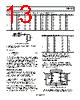
14 / 16 page  ADP1610 Rev. 0 | Page 14 of 16 DC-DC STEP-UP SWITCHING CONVERTER WITH TRUE SHUTDOWN Some battery-powered applications require very low standby current. The ADP1610 typically consumes 10 nA from the input, which makes it suitable for these applications. However, the output is connected to the input through the inductor and the rectifying diode, allowing load current draw from the input while shut down. The circuit in Figure 28 enables the ADP1610 to achieve output load disconnect at shutdown. To shut down the ADP1610 and disconnect the output from the input, drive the SD pin below 0.4 V. IN SD SS RT SW FB COMP CSS 22nF GND L 4.7 µH D1 ADP1610 5 6 3 2 7 8 1 4 CIN 10 µF B Q1 A Q1 FDC6331 CCOMP 150pF RCOMP 220k Ω COUT 10 µF R1 71.3k Ω OFF R2 10k Ω R3 10k Ω 3.3V 10V Figure 28. Step-Up Regulator with True Shutdown TFT LCD BIAS SUPPLY Figure 29 shows a power supply circuit for TFT LCD module applications. This circuit has +10 V, −5 V, and +22 V outputs. The +10 V is generated in the step-up configuration. The −5 V and +22 V are generated by the charge-pump circuit. During the step-up operation, the SW node switches between 10 V and ground (neglecting forward drop of the diode and on resistance of the switch). When the SW node is high, C5 charges up to 10 V. C5 holds its charge and forward-biases D8 to charge C6 to −10 V. The Zener diode, D9, clamps and regulates the output to −5 V. The VGH output is generated in a similar manner by the charge-pump capacitors, C1, C2, and C4. The output voltage is tripled and regulated down to 22 V by the Zener diode, D5. IN SD SS RT SW ON FB COMP CSS 22nF GND L 4.7 µH D1 D2 D3 BAV99 BAV99 BZT52C22 BZT52C5VIS BAV99 ADP1610 5 6 3 2 7 8 1 4 C1 10nF CIN 10 µF CCOMP 150pF RCOMP 220k Ω COUT 10 µF C2 1 µF C3 10 µF R1 71.3k Ω R2 10k Ω D5 D9 3.3V VGL –5V VGH 22V 10V D5 D4 D8 D7 C4 10nF R3 200 Ω C5 10nF C6 10 µF R4 200 Ω Figure 29. TFT LCD Bias Supply SEPIC POWER SUPPLY The circuit in Figure 30 shows the ADP1610 in a single-ended primary inductance converter (SEPIC) topology. This topology is useful for an unregulated input voltage, such as a battery- powered application in which the input voltage can vary between 2.7 V to 5 V, and the regulated output voltage falls within the input voltage range. The input and the output are dc-isolated by a coupling capaci- tor, C1. In steady state, the average voltage of C1 is the input voltage. When the ADP1610 switch turns on and the diode turns off, the input voltage provides energy to L1, and C1 provides energy to L2. When the ADP1610 switch turns off and the diode turns on, the energy in L1 and L2 is released to charge the output capacitor, COUT, and the coupling capacitor, C1, and to supply current to the load. 2.5V–5.5V 3.3V IN SD SS RT SW ON FB COMP CSS 22nF GND L1 4.7 µH 4.7 µH L2 ADP1610 5 6 3 2 7 8 1 4 CIN 10 µF CCOMP 1nF RCOMP 60k Ω COUT 10 µF C1 10 µF R1 16.8k Ω R2 10k Ω Figure 30. 3.3 V DC-DC Converter |
|
|
链接网址 |
| ALLDATASHEET是否为您带来帮助? [ DONATE ] |
关于 Alldatasheet | 广告服务 | 联系我们 | 隐私政策 | 数据表链接 | 链接交换 | 制造商名单 All Rights Reserved©Alldatasheet.com |
| Russian : Alldatasheetru.com | Korean : Alldatasheet.co.kr | Spanish : Alldatasheet.es | French : Alldatasheet.fr | Italian : Alldatasheetit.com Portuguese : Alldatasheetpt.com | Polish : Alldatasheet.pl | Vietnamese : Alldatasheet.vn Indian : Alldatasheet.in | Mexican : Alldatasheet.com.mx | British : Alldatasheet.co.uk | New Zealand : Alldatasheet.co.nz |
|
Family Site : ic2ic.com |
icmetro.com |
 Chinese ▼
 English
 Chinese
 German
 Japanese
 Russian
 Korean
 Spanish
 French
 Italian
 Portuguese
 Polish
 Vietnamese
 Indian
 Mexican
 British
 New Zealand