|
数据搜索系统,热门电子元器件搜索 |
|
|
数据搜索系统,热门电子元器件搜索 |
|
MCP1663 数据表(PDF) 12 Page - Microchip Technology |
|
|
|||||||||||||||||||||||||||||
MCP1663 数据表(HTML) 12 Page - Microchip Technology |
|
|
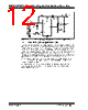
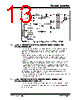
12 / 32 page  MCP1663 9V/12V/24V Output Boost Regulator Evaluation Board User’s Guide DS50002364A-page 12 2015 Microchip Technology Inc. FIGURE 1-1: Typical MCP1663 Boost Converter Two Alkaline Cells Input. 1.2.1 HIGH INPUT VOLTAGE CONFIGURATION The MCP1663 9V/12V/24V Output Boost Regulator Evaluation Board comes with two additional configurations that can be used to extend and overcome the typical low VIN voltage range, providing significantly more flexibility for applications powered from a higher input. The MCP1663 high-input voltage boost converter (the bottom circuit on the evaluation board) comes with two different solutions that can be used to extend the application's input voltage range beyond its typical values. For this circuit, VIN represents the voltage applied between the VIN and GND test points on the board and VDD represents the voltage that will be present on the MCP1663 input pin. • The first option used for driving the MCP1663’s low input (VDD) voltage internal circuitry is to use a linear dropout regulator (LDO) to step-down the application supply voltage (VIN) to 5V. • The second solution to limit the VIN voltage is to use a Zener diode regulator. The MCP1663 low input quiescent current keeps the LDO and the Zener diode circuitry power losses at a low level. µ VIN EN GND VFB SW VIN 2.4V - 3.2V VOUT 12V, >100 mA COUT 10 µF CIN 10 µF L 4.7 µH + 1.05 M 120 k + - OFF ON - D RT RB 20V, 500 mA |
|
链接网址 |
| ALLDATASHEET是否为您带来帮助? [ DONATE ] |
关于 Alldatasheet | 广告服务 | 联系我们 | 隐私政策 | 数据表链接 | 链接交换 | 制造商名单 All Rights Reserved©Alldatasheet.com |
| Russian : Alldatasheetru.com | Korean : Alldatasheet.co.kr | Spanish : Alldatasheet.es | French : Alldatasheet.fr | Italian : Alldatasheetit.com Portuguese : Alldatasheetpt.com | Polish : Alldatasheet.pl | Vietnamese : Alldatasheet.vn Indian : Alldatasheet.in | Mexican : Alldatasheet.com.mx | British : Alldatasheet.co.uk | New Zealand : Alldatasheet.co.nz |
|
Family Site : ic2ic.com |
icmetro.com |
 Chinese ▼
 English
 Chinese
 German
 Japanese
 Russian
 Korean
 Spanish
 French
 Italian
 Portuguese
 Polish
 Vietnamese
 Indian
 Mexican
 British
 New Zealand