|
数据搜索系统,热门电子元器件搜索 |
|
|
数据搜索系统,热门电子元器件搜索 |
|
MCP1663 数据表(PDF) 17 Page - Microchip Technology |
|
|
|||||||||||||||||||||||||||||
MCP1663 数据表(HTML) 17 Page - Microchip Technology |
|
|
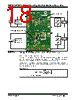
17 / 32 page  Installation and Operation 2015 Microchip Technology Inc. DS50002364A-page 17 2.2 GETTING STARTED The MCP1663 9V/12V/24V Output Boost Regulator Evaluation Board is fully assembled and tested to evaluate and demonstrate the MCP1663 product. This board requires the use of external laboratory supplies and load. 2.2.1 Power Input and Output Connection 2.2.1.1 POWERING THE MCP1663 9V/12V/24V OUTPUT BOOST REGULATOR EVALUATION BOARD The MCP1663 9V/12V/24V Output Boost Regulator Evaluation Board was designed to be used to evaluate the MCP1663 device. The package selected is SOT-23. Soldered test points are available for input voltage connections. Soldered test points are available to connect a load. The switch peak current limit will provide a safe maximum current value. The maximum output current for the converter will vary with input and output voltages; refer to Figure 2-3 or the MCP1663 data sheet for more information on the maximum output current. 2.2.1.2 BOARD POWER-UP PROCEDURE TOP CIRCUIT 1. Connect the input supply as shown in Figure 2-2. The input voltage should not be higher than 5.5V. 2. Connect system load to VOUT and GND terminals; maximum load varies with input and output voltage. Connect the (+) side of the load to VOUT and the negative (-) load to ground (GND). 3. The “VOUT SELECT” switch can be used to modify the output voltage between two values: - 9V, when the switch is in OFF position - 12V, when the switch is in ON position BOTTOM CIRCUIT 1. Connect the input supply as shown in Figure 2-2. 2. The MCP1663 can be used in the extended input voltage range 9V - 16V. 3. Connect system load to VOUT and GND terminals; maximum load varies with input and output voltage. Typically, the MCP1663 can supply a 24V output with 500 mA from a 12V input source at room temperature. Connect the (+) side of the load to VOUT and the negative (-) load to ground (GND). 4. There are two distinct methods that can be used to extend the input voltage range: - Using an LDO to provide the necessary low voltage (VDD) bias (jumper on J1 in “LDO” position) - Using a Zener diode (jumper on J1 in “Zener” position) |
|
链接网址 |
| ALLDATASHEET是否为您带来帮助? [ DONATE ] |
关于 Alldatasheet | 广告服务 | 联系我们 | 隐私政策 | 数据表链接 | 链接交换 | 制造商名单 All Rights Reserved©Alldatasheet.com |
| Russian : Alldatasheetru.com | Korean : Alldatasheet.co.kr | Spanish : Alldatasheet.es | French : Alldatasheet.fr | Italian : Alldatasheetit.com Portuguese : Alldatasheetpt.com | Polish : Alldatasheet.pl | Vietnamese : Alldatasheet.vn Indian : Alldatasheet.in | Mexican : Alldatasheet.com.mx | British : Alldatasheet.co.uk | New Zealand : Alldatasheet.co.nz |
|
Family Site : ic2ic.com |
icmetro.com |
 Chinese ▼
 English
 Chinese
 German
 Japanese
 Russian
 Korean
 Spanish
 French
 Italian
 Portuguese
 Polish
 Vietnamese
 Indian
 Mexican
 British
 New Zealand