|
数据搜索系统,热门电子元器件搜索 |
|
|
数据搜索系统,热门电子元器件搜索 |
|
AD8392ACP-R2 数据表(PDF) 13 Page - Analog Devices |
|
|
|||||||||||||||||||||||||||||
AD8392ACP-R2 数据表(HTML) 13 Page - Analog Devices |
|
|
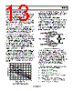
13 / 16 page  AD8392 Rev. 0 | Page 13 of 16 THERMAL CONSIDERATIONS When using a quad, high output current amplifier, such as the AD8392, special consideration should be given to system level thermal design. In applications such as ADSL/ADSL2+, the AD8392 could be required to dissipate as much as 1.4 W or more on chip. Under these conditions, particular attention should be paid to the thermal design in order to maintain safe operating temperatures on the die. To aid in the thermal design, the thermal information in the Thermal Resistance section can be combined with what follows here. The information in Table 4 and Figure 3 is based on a standard JEDEC 4-layer board and a maximum die temperature of 150°C. To provide additional guidance and design suggestions, a thermal study was performed under a set of conditions more closely aligned with an actual ADSL/ADSL2+ application. In a typical ADSL/ADSL2+ line card, component density usu- ally dictates that most of the copper plane used for thermal dissipation be internal. Additionally, each ADSL/ADSL2+ port may be allotted only 1 square inch, or even less, of board space. For these reasons, a special thermal test board was constructed for this study. The 4-layer board measured approximately 4 inches × 4 inches and contained two internal 1 oz copper ground planes, each measuring 2 inches × 3 inches. The top layer contained signal traces and an exposed copper strip ¼ inch × 3 inches to accommodate heat sinking, with no other copper on the top or bottom of the board. Three 28-lead TSSOPs were placed on the board representing six ADSL channels, or one channel per square inch of copper, with each channel dissipating 700 mW on-chip (1.4 W per package). The die temperature is then measured in still air and in a wind tunnel with calibrated airflow of 100 LFM, 200 LFM, and 400 LFM. Figure 36 shows the power dissipation versus the ambient temperature for each airflow condition. The figure assumes a maximum die temperature of 135°C. No heat sink was used. 1.0 1.5 2.0 2.5 3.0 3.5 4.0 4.5 5 15 25354555657585 AMBIENT TEMPERATURE ( °C) TJ = 135°C STILL AIR 100LFM 200LFM 400LFM Figure 36. Power Dissipation vs. Ambient Temperature and Air Flow 28-Lead TSSOP/EP This data is only provided as guidance to assist in the thermal design process. Due diligence should be performed with regards to power dissipation because there are many factors that can affect thermal performance. TYPICAL ADSL/ADSL2+ APPLICATION In a typical ADSL/ADSL2+ application, a differential line driver is used to take the signal from the analog front end (AFE) and drive it onto the twisted pair telephone line. Referring to the typical circuit representation in Figure 37, the differential input appears at VIN+ and VIN− from the AFE, while the differential output is transformer coupled to the telephone line at tip and ring. The common-mode operating point, generally midway between the supplies, is set through VCOM. R4 R4 R3 R3 Rm R2 R1 R2 VCOM 1:N TIP RING ROUT RIN Rm VOA VOA VP VP RBIAS RBIAS VIN– VIN+ Figure 37. Typical ADSL/ADSL2+ Application Circuit In ADSL/ADSL2+ applications, it is common practice to conserve power by using positive feedback to synthesize the output resistance, thereby lowering the required ohmic value of the line matching resistors, Rm. The circuit in Figure 37 is somewhat unique in that the positive feedback introduced via R3 has the effect of synthesizing the input resistance as well. The following definitions and equations can be used to calculate the resistor values necessary to obtain the desired gain, input resistance, and output resistance for a given application. For simplicity the following calculations assume a lossless transformer. The following values are used in the design equations and are assumed already known or chosen by the designer. VIN Differential input voltage RIN Desired differential input resistance N Transformer turns ratio VLINE Differential output voltage at tip and ring Rm Each is typically 5% to 15% of the transformer reflected line impedance R2 Recommended in the amplifier data sheet VP Voltage at the + inputs to the amplifier, approximately ½ VIN (must be less than VIN for positive input resistance) RL Transformer reflected line impedance |
|
|
链接网址 |
| ALLDATASHEET是否为您带来帮助? [ DONATE ] |
关于 Alldatasheet | 广告服务 | 联系我们 | 隐私政策 | 数据表链接 | 链接交换 | 制造商名单 All Rights Reserved©Alldatasheet.com |
| Russian : Alldatasheetru.com | Korean : Alldatasheet.co.kr | Spanish : Alldatasheet.es | French : Alldatasheet.fr | Italian : Alldatasheetit.com Portuguese : Alldatasheetpt.com | Polish : Alldatasheet.pl | Vietnamese : Alldatasheet.vn Indian : Alldatasheet.in | Mexican : Alldatasheet.com.mx | British : Alldatasheet.co.uk | New Zealand : Alldatasheet.co.nz |
|
Family Site : ic2ic.com |
icmetro.com |
 Chinese ▼
 English
 Chinese
 German
 Japanese
 Russian
 Korean
 Spanish
 French
 Italian
 Portuguese
 Polish
 Vietnamese
 Indian
 Mexican
 British
 New Zealand