|
数据搜索系统,热门电子元器件搜索 |
|
|
数据搜索系统,热门电子元器件搜索 |
|
ADL5306ACP-R2 数据表(PDF) 13 Page - Analog Devices |
|
|
|||||||||||||||||||||||||||||
ADL5306ACP-R2 数据表(HTML) 13 Page - Analog Devices |
|
|
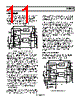
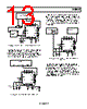
13 / 16 page  ADL5306 Rev. 0 | Page 13 of 16 R1 R2 1k Ω 1k Ω 1nF 1nF NC INPT VREF IREF SCAL BFIN VPOS 0.1 µF +VS COMM COMM COMM COMM VNEG VNEG VSUM VOUT VLOG 1 2 3 4 56 78 9 10 11 12 13 14 15 16 ADL5306 03727-0-026 AD8138 EVALUATION BOARD HP3577A NETWORK ANALYZER +IN B A OUTPUT INPUT R INPUT A INPUT B POWER SPLITTER Figure 26. Configuration for Logarithmic Amplifier Bandwidth Measurement Figure 26 shows the configuration used for frequency response measurements of the logarithmic amplifier section. The AD8138 output is offset to 1.5 V dc and modulated to a depth of 5% at frequency. R1 is chosen (over a wide range of values up to 1.0 GΩ) to provide IPD. The buffer is used to deload VLOG. R1 200k Ω 1k Ω 1nF 1k Ω 1nF NC INPT VREF IREF SCAL BFIN VPOS 0.1 µF ALKALINE "D" CELL ALKALINE "D" CELL COMM COMM COMM COMM VNEG VNEG VSUM VOUT VLOG 1 2 3 4 567 8 9 10 11 12 13 14 15 16 ADL5306 03727-0-027 HP89410A SOURCE TRIGGER CHANNEL 1 CHANNEL 2 Figure 27. Configuration for Noise Spectral Density Measurement The configuration of Figure 27 is used to measure the noise performance. Batteries provide both the supply voltage and the input current in order to minimize the introduction of spurious noise and ground loop effects. The entire evaluation system, including the current setting resistors, is mounted in a closed aluminum enclosure to provide additional shielding to external noise sources. R1 200k Ω 1k Ω 1nF 1k Ω 50k Ω 1nF NC INPT VREF IREF SCAL BFIN VPOS 0.1 µF +VS COMM COMM COMM COMM VNEG VNEG VSUM VOUT VLOG 1 2 3 4 56 78 9 10 11 12 13 14 15 16 ADL5306 03727-0-028 TDS5104 CH 1 LeCROY 9210 CH A 9213 Figure 28. Configuration for Logarithmic Amplifier Pulse Response Measurement Figure 28 shows the setup used to make the pulse response measurements. As with the bandwidth measurement, VLOG is connected directly to BFIN and the buffer amplifier is configured for a gain of 1. The buffer’s output is connected through a short cable to the TDS5104 scope, with the input impedance set to 1 MΩ. The LeCroy’s output is offset to create the initial pedestal current for a given R1 value. The pulse then creates a 1-decade current step. |
|
|
链接网址 |
| ALLDATASHEET是否为您带来帮助? [ DONATE ] |
关于 Alldatasheet | 广告服务 | 联系我们 | 隐私政策 | 数据表链接 | 链接交换 | 制造商名单 All Rights Reserved©Alldatasheet.com |
| Russian : Alldatasheetru.com | Korean : Alldatasheet.co.kr | Spanish : Alldatasheet.es | French : Alldatasheet.fr | Italian : Alldatasheetit.com Portuguese : Alldatasheetpt.com | Polish : Alldatasheet.pl | Vietnamese : Alldatasheet.vn Indian : Alldatasheet.in | Mexican : Alldatasheet.com.mx | British : Alldatasheet.co.uk | New Zealand : Alldatasheet.co.nz |
|
Family Site : ic2ic.com |
icmetro.com |
 Chinese ▼
 English
 Chinese
 German
 Japanese
 Russian
 Korean
 Spanish
 French
 Italian
 Portuguese
 Polish
 Vietnamese
 Indian
 Mexican
 British
 New Zealand