|
数据搜索系统,热门电子元器件搜索 |
|
|
数据搜索系统,热门电子元器件搜索 |
|
ADL5306ACP-R2 数据表(PDF) 14 Page - Analog Devices |
|
|
|||||||||||||||||||||||||||||
ADL5306ACP-R2 数据表(HTML) 14 Page - Analog Devices |
|
|
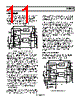
14 / 16 page  ADL5306 Rev. 0 | Page 14 of 16 EVALUATION BOARD An evaluation board is available for the ADL5306, the schematic of which is shown in 29. It can be configured for a wide variety of experiments. The buffer gain is factory-set to unity, providing a slope of 200 mV/dec, and the intercept is set to 1 nA. Table 4 describes the various configuration options. Table 4. Evaluation Board Configuration Options Component Function Default Conditions P1 Supply Interface. Provides access to supply pins VNEG, COMM, and VPOS. P1 = Installed P2, R8, R9, R10, R18 Monitor Interface. By adding 0 Ω resistors to R8, R9, R10, and R18, the VREF, VSUM, VOUT, and VLOG pin voltages can be monitored using a high impedance probe. P2 = Not Installed R8 = R9 = R10 = Open (Size 0603) R18 = Open (Size 0603) R2, R3, R4, R6, R11, R14, C2, C7, C9, C10 Buffer Amplifier/Output Interface. The logarithmic slope of the ADL5306 can be altered using the buffer’s gain- setting resistors, R2 and R3. R4, R6, R11, R14, C2, C7, C9, and C10 are provided for a variety of filtering applications. R2 = R6 = 0 Ω (Size 0603) R3 = R4 = Open (Size 0603) R11 = R14 = 0 Ω (Size 0603) C2 = C7 = Open (Size 0603) C9 = C10 = Open (Size 0603) VLOG = VOUT = Installed R1, R19 Intercept Adjustment. The voltage dropped across resistor R1 determines the intercept reference current, nominally set to 10 µA using a 200 kΩ 1% resistor. R1 = 200 kΩ (Size 0603) R19 = 0 Ω (Size 0603) R12, R15, C3, C4, C5, C6 Supply Decoupling C3 = C4 = 0.01 µF (Size 0603) C5 = C6 = 0.1 µF (Size 0603) R12 = R15 = 0 Ω (Size 0603) C11 Filtering VSUM C11 = 1 nF (Size 0603) R13, R16, C1, C8 Input Compensation. Provides essential HF compensation at the input pins, INPT and IREF. R13 = R16 = 1 kΩ (Size 0603) C1 = C8 = 1 nF (Size 0603) IREF, INPT, PD, LK1, R5 Input Interface. The test board is configured to accept a current through the SMA connector labeled INPT. An SC style packaged photodiode can be used in place of the INPT SMA for optical interfacing. By removing R1 and adding a 0 Ω short for R5, a second current can be applied to the IREF input (also SMA) for evaluating the ADL5306 in log-ratio applications. IREF = INPT = Installed PD = Not Installed LK1 = Installed R5 = Open (Size 0603) J1 SC Style Photodiode J1 = Open |
|
|
链接网址 |
| ALLDATASHEET是否为您带来帮助? [ DONATE ] |
关于 Alldatasheet | 广告服务 | 联系我们 | 隐私政策 | 数据表链接 | 链接交换 | 制造商名单 All Rights Reserved©Alldatasheet.com |
| Russian : Alldatasheetru.com | Korean : Alldatasheet.co.kr | Spanish : Alldatasheet.es | French : Alldatasheet.fr | Italian : Alldatasheetit.com Portuguese : Alldatasheetpt.com | Polish : Alldatasheet.pl | Vietnamese : Alldatasheet.vn Indian : Alldatasheet.in | Mexican : Alldatasheet.com.mx | British : Alldatasheet.co.uk | New Zealand : Alldatasheet.co.nz |
|
Family Site : ic2ic.com |
icmetro.com |
 Chinese ▼
 English
 Chinese
 German
 Japanese
 Russian
 Korean
 Spanish
 French
 Italian
 Portuguese
 Polish
 Vietnamese
 Indian
 Mexican
 British
 New Zealand