|
数据搜索系统,热门电子元器件搜索 |
|
|
数据搜索系统,热门电子元器件搜索 |
|
DFE252012F-R47M 数据表(PDF) 115 Page - Analog Devices |
|
|
|||||||||||||||||||||||||||||
DFE252012F-R47M 数据表(HTML) 115 Page - Analog Devices |
|
|
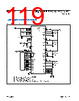
115 / 122 page  COUT1 COUT1 COUT1 COUT1 COUT1 COUT1 COUT4 COUT4 COUT4 COUT4 COUT4 COUT4 COUT2 COUT2 COUT2 COUT2 COUT2 COUT2 COUT3 COUT3 COUT3 COUT3 COUT3 COUT3 CSYS CALT_IN CVIO CBST4 CBST3 OUT1 OUT2 OUT3 OUT4 LX1 PGND PGND AGND NOTE 1: INTERNAL SIGNALS ARE ROUTED OUT ON THE SECOND AND THIRD LAYERS OF THE PCB. SEE THE EV KIT LAYOUT FILES FOR AN EXAMPLE. AGND CBST1 CBST2 SCL SDA CE INNER BUMPS (SEE NOTE 1) Figure 15. PCB Layout Example Unused Outputs When an application has unused buck outputs, follow the guidelines below: ● Connect the unused inputs (INx) to the SYS. ● Leave the unused LXx and the BSTx pins unconnected (open). ● Connect the unused SNSxP and SNSxN inputs to ground (AGND). ● Connect the PGNDx pins to ground. ● Do not enable the unused buck outputs. The slave phases configured under master controllers must be connected according to Table 6. If an unused buck output MAX77542 16VIN/16A, Quad-Phase High-Efficiency Buck Converter www.analog.com Analog Devices | 115 |
|
链接网址 |
| ALLDATASHEET是否为您带来帮助? [ DONATE ] |
关于 Alldatasheet | 广告服务 | 联系我们 | 隐私政策 | 数据表链接 | 链接交换 | 制造商名单 All Rights Reserved©Alldatasheet.com |
| Russian : Alldatasheetru.com | Korean : Alldatasheet.co.kr | Spanish : Alldatasheet.es | French : Alldatasheet.fr | Italian : Alldatasheetit.com Portuguese : Alldatasheetpt.com | Polish : Alldatasheet.pl | Vietnamese : Alldatasheet.vn Indian : Alldatasheet.in | Mexican : Alldatasheet.com.mx | British : Alldatasheet.co.uk | New Zealand : Alldatasheet.co.nz |
|
Family Site : ic2ic.com |
icmetro.com |
 Chinese ▼
 English
 Chinese
 German
 Japanese
 Russian
 Korean
 Spanish
 French
 Italian
 Portuguese
 Polish
 Vietnamese
 Indian
 Mexican
 British
 New Zealand