|
数据搜索系统,热门电子元器件搜索 |
|
|
数据搜索系统,热门电子元器件搜索 |
|
AD8045ACP-R2 数据表(PDF) 17 Page - Analog Devices |
|
|
|||||||||||||||||||||||||||||
AD8045ACP-R2 数据表(HTML) 17 Page - Analog Devices |
|
|
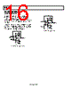
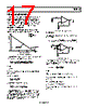
17 / 24 page  AD8045 Rev. A | Page 17 of 24 THEORY OF OPERATION The AD8045 is a high speed voltage feedback amplifier fabri- cated on ADI’s second generation eXtra Fast Complementary Bipolar (XFCB) process. An H-bridge input stage is used to attain a 1400 V/µs slew rate and low distortion in addition to a low 3 nV/√Hz input voltage noise. Supply current and offset voltage are laser trimmed for optimum performance. FREQUENCY RESPONSE The AD8045’s open-loop response over frequency can be approximated by the integrator response shown in Figure 63. fCROSSOVER = 400MHz FREQUENCY (MHz) 0 1 10 100 f 1000 VOUT/VIN = fCROSSOVER VIN VOUT Figure 63. Open-Loop Response The closed-loop transfer function for the noninverting configu- ration is shown in Figure 64 and is written as () G CROSSOVER G F F G CROSSOVER IN OUT R f R R R R f V V × × + + + × × = π 2 s ) ( π 2 where: s is (2 πj)f. fCROSSOVER is the frequency where the amplifier’s open-loop gain equals 1 (0 dB). DC gain is therefore () G F G IN OUT R R R V V + = Closed-loop −3 dB bandwidth equals () F G G CROSSOVER IN OUT R R R f V V + × = The closed-loop bandwidth is inversely proportional to the noise gain of the op amp circuit, (RF + RG)/RG. This simple model can be used to predict the −3 dB bandwidth for noise gains above +2. The actual bandwidth of circuits with noise gains at or below +2 is higher due to the influence of other poles present in the real op amp. RG RF VIN VOUT RS +– Figure 64. Noninverting Configuration DC ERRORS Figure 65 shows the dc error contributions. The total output error voltage is ⎟ ⎠ ⎞ ⎜ ⎝ ⎛ + + + ⎟ ⎠ ⎞ ⎜ ⎝ ⎛ + − = − + G F G OS F B G F G S B (ERROR) OUT R R R V R I R R R R I V RG RF VOS VOUT RS +– IB+ IB– Figure 65. Amplifier DC Errors The voltage error due to IB+ and IB− is minimized if RS = RF||RG. To include the effects of common-mode and power supply rejection, model VOS as CMR V PSR V V V CM S OS OS nom ∆ + ∆ + = where: nom os V is the offset voltage at nominal conditions. ΔVS is the change in the power supply voltage from nominal conditions. PSR is the power supply rejection. CMR is the common-mode rejection. ΔVCM is the change in common-mode voltage from nominal conditions. |
|
|
链接网址 |
| ALLDATASHEET是否为您带来帮助? [ DONATE ] |
关于 Alldatasheet | 广告服务 | 联系我们 | 隐私政策 | 数据表链接 | 链接交换 | 制造商名单 All Rights Reserved©Alldatasheet.com |
| Russian : Alldatasheetru.com | Korean : Alldatasheet.co.kr | Spanish : Alldatasheet.es | French : Alldatasheet.fr | Italian : Alldatasheetit.com Portuguese : Alldatasheetpt.com | Polish : Alldatasheet.pl | Vietnamese : Alldatasheet.vn Indian : Alldatasheet.in | Mexican : Alldatasheet.com.mx | British : Alldatasheet.co.uk | New Zealand : Alldatasheet.co.nz |
|
Family Site : ic2ic.com |
icmetro.com |
 Chinese ▼
 English
 Chinese
 German
 Japanese
 Russian
 Korean
 Spanish
 French
 Italian
 Portuguese
 Polish
 Vietnamese
 Indian
 Mexican
 British
 New Zealand