|
数据搜索系统,热门电子元器件搜索 |
|
|
数据搜索系统,热门电子元器件搜索 |
|
AD8045ACP-R2 数据表(PDF) 23 Page - Analog Devices |
|
|
|||||||||||||||||||||||||||||
AD8045ACP-R2 数据表(HTML) 23 Page - Analog Devices |
|
|
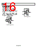
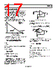
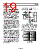
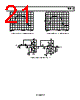
23 / 24 page  AD8045 Rev. A | Page 23 of 24 EXPOSED PADDLE The AD8045 features an exposed paddle, which lowers the thermal resistance by 25% compared to a standard SOIC plastic package. The exposed paddle of the AD8045 is internally con- nected to the negative power supply pin. Therefore, when laying out the board, the exposed paddle must either be connected to the negative power supply or left floating (electrically isolated). Soldering the exposed paddle to the negative power supply metal ensures maximum thermal transfer. Figure 74 and Figure 75 show the proper layout for connecting the SOIC and LFCSP exposed paddle to the negative supply. Figure 74. SOIC Exposed Paddle Layout The use of thermal vias or “heat pipes” can also be incorporated into the design of the mounting pad for the exposed paddle. These additional vias help to lower the overall theta junction to ambient (θJA). Using a heavier weight copper on the surface to which the amplifier’s exposed paddle is soldered can greatly reduce the overall thermal resistance “seen” by the AD8045. Figure 75. LFCSP Exposed Paddle Layout For existing designs that want to incorporate the AD8045, electrically isolating the exposed paddle is another option. If the exposed paddle is electrically isolated, the thermal dissipation is primarily through the leads, and the thermal resistance of the package now approaches 125°C/W, the standard SOIC θJA. However, a thermally conductive and electrically isolated pad material may be used. A thermally conductive spacer, such as the Bergquist Company’s Sil-Pad, is an excellent solution to this problem. Figure 76 shows a typical implementation using thermal pad material. THERMAL CONDUCTIVE INSULATOR Figure 76. SOIC with Thermal Conductive Pad Material The thermal pad provides high thermal conductivity but isolates the exposed paddle from ground or other potential. It is recommended, when possible, to solder the paddle to the nega- tive power supply plane or trace for maximum thermal transfer. Note that soldering the paddle to ground shorts the negative power supply to ground and can cause irreparable damage to the AD8045. DRIVING CAPACITIVE LOADS In general, high speed amplifiers have a difficult time driving capacitive loads. This is particularly true in low closed-loop gains, where the phase margin is the lowest. The difficulty arises because the load capacitance, CL, forms a pole with the output resistance, RO, of the amplifier. The pole can be described by the equation L O P C R f 2π 1 = If this pole occurs too close to the unity gain crossover point, the phase margin degrades. This is due to the additional phase loss associated with the pole. The AD8045 output can drive 18 pF of load capacitance directly, in a gain of +2 with 30% overshoot, as shown in Figure 37. Larger capacitance values can be driven but must use a snub- bing resistor (RSNUB) at the output of the amplifier, as shown in Figure 61 and Figure 62. Adding a small series resistor, RSNUB, creates a zero that cancels the pole introduced by the load capacitance. Typical values for RSNUB can range from 25 Ω to 50 Ω. The value is typically arrived at empirically and based on the circuit requirements. |
|
|
链接网址 |
| ALLDATASHEET是否为您带来帮助? [ DONATE ] |
关于 Alldatasheet | 广告服务 | 联系我们 | 隐私政策 | 数据表链接 | 链接交换 | 制造商名单 All Rights Reserved©Alldatasheet.com |
| Russian : Alldatasheetru.com | Korean : Alldatasheet.co.kr | Spanish : Alldatasheet.es | French : Alldatasheet.fr | Italian : Alldatasheetit.com Portuguese : Alldatasheetpt.com | Polish : Alldatasheet.pl | Vietnamese : Alldatasheet.vn Indian : Alldatasheet.in | Mexican : Alldatasheet.com.mx | British : Alldatasheet.co.uk | New Zealand : Alldatasheet.co.nz |
|
Family Site : ic2ic.com |
icmetro.com |
 Chinese ▼
 English
 Chinese
 German
 Japanese
 Russian
 Korean
 Spanish
 French
 Italian
 Portuguese
 Polish
 Vietnamese
 Indian
 Mexican
 British
 New Zealand