|
数据搜索系统,热门电子元器件搜索 |
|
|
数据搜索系统,热门电子元器件搜索 |
|
ADCMP580BCP-R2 数据表(PDF) 11 Page - Analog Devices |
|
|
|||||||||||||||||||||||||||||
ADCMP580BCP-R2 数据表(HTML) 11 Page - Analog Devices |
|
|
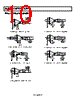
11 / 16 page  ADCMP580/ADCMP581/ADCMP582 Rev. 0 | Page 11 of 16 APPLICATION INFORMATION POWER/GROUND LAYOUT AND BYPASSING The ADCMP58x family of comparators is designed for very high speed applications. Consequently, high speed design techniques must be used to achieve the specified performance. It is critically important to use low impedance supply planes, particularly for the negative supply (VEE), the output supply plane (VCCO), and the ground plane (GND). Individual supply planes are recommended as part of a multilayer board. Provid- ing the lowest inductance return path for the switching currents ensures the best possible performance in the target application. It is also important to adequately bypass the input and output supplies. A 1 μF electrolytic bypass capacitor should be placed within several inches of each power supply pin to ground. In addition, multiple high quality 0.1 μF bypass capacitors should be placed as close as possible to each of the VEE, VCCI, and VCCO supply pins and should be connected to the GND plane with redundant vias. High frequency bypass capacitors should be carefully selected for minimum inductance and ESR. Parasitic layout inductance should be strictly avoided to maximize the effectiveness of the bypass at high frequencies. ADCMP58x FAMILY OF OUTPUT STAGES Specified propagation delay dispersion performance is achieved by using proper transmission line terminations. The outputs of the ADCMP580 family comparators are designed to directly drive 400 mV into 50 Ω cable or microstrip/stripline transmis- sion lines terminated with 50 Ω referenced to the proper return. The CML output stage is shown in the simplified schematic diagram in Figure 24. Each output is back-terminated with 50 Ω for best transmission line matching. The outputs of the ADCMP581/ADCMP582 are illustrated in Figure 25; they should be terminated to −2 V for ECL outputs of ADCMP581 and VCCO − 2 V for PECL outputs of ADCMP582. As an alter- native, Thevenin equivalent termination networks may also be used. If these high speed signals must be routed more than a centimeter, then either microstrip or stripline techniques are required to ensure proper transition times and to prevent excessive output ringing and pulse width-dependent propagation delay dispersion. Q 16mA 50 Ω 50 Ω Q GND VEE Figure 24. Simplified Schematic Diagram of the ADCMP580 CML Output Stage GND / Vcco VEE Q Q Figure 25. Simplified Schematic Diagram of the ADCMP581/ADCMP582 ECL/PECL Output Stage USING/DISABLING THE LATCH FEATURE The latch inputs (LE/LE) are active low for latch mode and are internally terminated with 50 Ω resistors to the VTT pin. When using the ADCMP580, VTT should be connected to ground. When using the ADCMP581, VTT should be connected to −2 V. When using the ADCMP582, VTT should be connected externally to VCCO − 2 V, preferably with its own low inductance plane. When using the ADCMP580/ADCMP582, the latch function can be disabled by connecting the LE pin to VEE with an external pull-down resistor and leaving the LE pin discon- nected. To prevent excessive power dissipation, the resistor should be 1.5 kΩ for the ADCMP580 and 1 kΩ for the ADCMP582. When using the ADCMP581 comparators, the latch can be disabled by connecting the LE pin to GND with an external 450 Ω resistor and leaving the LE pin disconnected. The idea is to create an approximate 0.5 V offset using the internal resistor as half of the voltage divider. The VTT pin should be connected as recommended. |
|
|
链接网址 |
| ALLDATASHEET是否为您带来帮助? [ DONATE ] |
关于 Alldatasheet | 广告服务 | 联系我们 | 隐私政策 | 数据表链接 | 链接交换 | 制造商名单 All Rights Reserved©Alldatasheet.com |
| Russian : Alldatasheetru.com | Korean : Alldatasheet.co.kr | Spanish : Alldatasheet.es | French : Alldatasheet.fr | Italian : Alldatasheetit.com Portuguese : Alldatasheetpt.com | Polish : Alldatasheet.pl | Vietnamese : Alldatasheet.vn Indian : Alldatasheet.in | Mexican : Alldatasheet.com.mx | British : Alldatasheet.co.uk | New Zealand : Alldatasheet.co.nz |
|
Family Site : ic2ic.com |
icmetro.com |
 Chinese ▼
 English
 Chinese
 German
 Japanese
 Russian
 Korean
 Spanish
 French
 Italian
 Portuguese
 Polish
 Vietnamese
 Indian
 Mexican
 British
 New Zealand