|
数据搜索系统,热门电子元器件搜索 |
|
|
数据搜索系统,热门电子元器件搜索 |
|
AD8137YCP-R2 数据表(PDF) 22 Page - Analog Devices |
|
|
|||||||||||||||||||||||||||||
AD8137YCP-R2 数据表(HTML) 22 Page - Analog Devices |
|
|
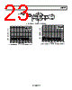
22 / 24 page  AD8137 Rev. B | Page 22 of 24 This example shows that when RF and RG are large compared to RT, the gain reduction produced by the increase in RG is essentially cancelled by the increase in the Thevenin voltage caused by RT being greater than the output resistance of the signal source. In general, as RF and RG become smaller in termi- nated applications, RF needs to be increased to compensate for the increase in RG. AD8137 + – 8 2 1 6 3 4 0V 2V p-p RT 52.3 Ω 5 + – VOCM 1k Ω 1.02k Ω 1k Ω 1k Ω 0.1 µF 0.1 µF +5V –5V VIN SIGNAL SOURCE 50 Ω When generating the typical performance characteristics data, the measurements were calibrated to take the effects of the terminations on closed-loop gain into account. Power Down The AD8137 features a PD pin that can be used to minimize the quiescent current consumed when the device is not being used. PD is asserted by applying a low logic level to Pin 7. The thresh- old between high and low logic levels is nominally 1.1 V above the negative supply rail. See the Specification tables (Table 1 to Table 3) for the threshold limits. Figure 66. AD8137 with Terminated Input The 52.3 Ω termination resistor, RT, in parallel with the 1 kΩ input resistance of the AD8137 circuit, yields an overall input resistance of 50 Ω that is seen by the signal source. In order to have matched feedback loops, each loop must have the same RG if it has the same RF. In the input (upper) loop, RG is equal to the 1 kΩ resistor in series with the (+) input plus the parallel combination of RT and the source resistance of 50 Ω. In the upper loop, RG is therefore equal to 1.03 kΩ. The closest standard value is 1.02 kΩ and is used for RG in the lower loop. DRIVING AN ADC WITH GREATER THAN 12-BIT PERFORMANCE Since the AD8137 is suitable for 12-bit systems, it is desirable to measure the performance of the amplifier in a system with greater than 12-bit linearity. In particular, the effective number of bits, ENOB, is most interesting. The AD7687, 16-bit, 250 KSPS ADC’s performance makes it an ideal candidate for showcasing the 12-bit performance of the AD8137. Things become more complicated when it comes to determining the feedback resistor values. The amplitude of the signal source generator VIN is two times the amplitude of its output signal when terminated in 50 Ω. Therefore, a 2 V p-p terminated amplitude is produced by a 4 V p-p amplitude from VS. The Thevenin equivalent circuit of the signal source and RT must be used when calculating the closed-loop gain because RG in the upper loop is split between the 1 kΩ resistor and the Thevenin resistance looking back toward the source. The Thevenin voltage of the signal source is greater than the signal source output voltage when terminated in 50 Ω because RT must always be greater than 50 Ω. In this case, RT is 52.3 Ω and the Thevenin voltage and resistance are 2.04 V p-p and 25.6 Ω, respectively. For this application, the AD8137 is set in a gain of two and driven single-ended through a 20 kHz band-pass filter, while the output is taken differentially to the input of the AD7687 (see Figure 67). This circuit has mismatched RG impedances and, therefore, has a dc offset at the differential output. It is included as a test circuit to illustrate the performance of the AD8137. Actual application circuits should have matched feedback networks. For an AD7687 input range up to −1.82 dBFS, the AD8137 power supply is a single 5 V applied to VS+ with VS− tied to ground. To increase the AD7687 input range to −0.45 dBFS, the AD8137 supplies are increased to +6 V and −1 V. In both cases, the VOCM pin is biased with 2.5 V and the PD pin is left floating. All voltage supplies are decoupled with 0.1 µF capacitors. Figure 68 and Figure 69 show the performance of the −1.82 dBFS setup and the −0.45 dBFS setup, respectively. Now the upper input branch can be viewed as a 2.04 V p-p source in series with 1.03 kΩ. Since this is to be a unity-gain application, a 2 V p-p differential output is required, and RF must therefore be 1.03 kΩ × (2/2.04) = 1.01 kΩ ≈ 1 kΩ. |
|
|
链接网址 |
| ALLDATASHEET是否为您带来帮助? [ DONATE ] |
关于 Alldatasheet | 广告服务 | 联系我们 | 隐私政策 | 数据表链接 | 链接交换 | 制造商名单 All Rights Reserved©Alldatasheet.com |
| Russian : Alldatasheetru.com | Korean : Alldatasheet.co.kr | Spanish : Alldatasheet.es | French : Alldatasheet.fr | Italian : Alldatasheetit.com Portuguese : Alldatasheetpt.com | Polish : Alldatasheet.pl | Vietnamese : Alldatasheet.vn Indian : Alldatasheet.in | Mexican : Alldatasheet.com.mx | British : Alldatasheet.co.uk | New Zealand : Alldatasheet.co.nz |
|
Family Site : ic2ic.com |
icmetro.com |
 Chinese ▼
 English
 Chinese
 German
 Japanese
 Russian
 Korean
 Spanish
 French
 Italian
 Portuguese
 Polish
 Vietnamese
 Indian
 Mexican
 British
 New Zealand