|
数据搜索系统,热门电子元器件搜索 |
|
|
数据搜索系统,热门电子元器件搜索 |
|
ADL5904ACPZN-R7 数据表(PDF) 18 Page - Analog Devices |
|
|
|||||||||||||||||||||||||||||
ADL5904ACPZN-R7 数据表(HTML) 18 Page - Analog Devices |
|
|
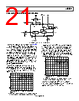
18 / 27 page  ADL5904 Data Sheet Rev. B | Page 18 of 27 THEORY OF OPERATION The ADL5904 is a true rms detector with a 45 dB measurement range at 1.9 GHz with useable range up to 6 GHz. It features no error ripple over its range, low temperature drift, and very low power consumption. Temperature stability of the rms output measurements provides ≤±0.5 dB error (typical) over the temperature range of −40°C to +85°C at up to 3.5 GHz. The measurement output voltage scales linearly in decibels with a slope of typically 36.9 mV/dB at 1.9 GHz. The core rms processing of the ADL5904 uses a proprietary multistage technique that provides accuracy for complex modulation signals irrespective of the crest factor of the input signal. An integrating filter capacitor at the CRMS pin performs the square domain averaging. R ENVELOPE DETECTOR RMS + – Q S ADL5904 VPOS GND VRMS RST Q RFIN VIN– DECL ENBL CRMS Q 1 11 DNC 2 3 6 8 4 4 5 7 12 13 Q 10 9 16 15 VCAL Figure 43. Functional Block Diagram The output of the first signal processing stage (the envelope detector), also drives the noninverting input of a threshold detecting comparator. The inverting input of this comparator is typically driven by a fixed external dc voltage. When the output of the envelope detector exceeds the voltage on the inverting input of the comparator, the comparator goes high. This excursion is then captured and held by an SR flip flop. The state of this flip flop is then held until the level sensitive RST pin is taken high. BASIC CONNECTIONS FOR RMS MEASUREMENT The ADL5904 requires a single supply of 3.3 V. The supply is connected to the VPOS supply pins. Decouple these pins using two capacitors with values equal or similar to those shown in the Figure 44. Place these capacitors as close to Pin 5 as possible. Connect Pin 11 (GND) and the exposed pad to a ground plane with low electrical and thermal impedance. A single-ended input at the RFIN pin drives the ADL5904. Because the input is dc-coupled, an external ac coupling capacitor must be used. A 470 nF capacitor is recommended for applications that require frequency coverage from 6 GHz down to tens of kilohertz. For applications that do not need such low frequency coverage, a larger value of capacitance can be used. In addition to the ac-coupling capacitor, an external 82.5 Ω shunt resistor is required to provide a wideband input match. Figure 13 shows a comparison of the input return loss, with and without the external shunt resistor. The rms measurement voltage is available on the VRMS pin. Place a 10 nF load capacitor on this pin. The DECL pin provides a bypass capacitor connection for an on-chip regulator. The DECL pin is connected to ground with a 4.02 Ω resistor and a 0.1 µF capacitor. The CRMS pin is the averaging node for the rms computation. Place an rms averaging capacitor between the CRMS and DECL pins. For information on choosing the CRMS capacitor, see the Choosing a Value for CRMS section. Using smaller values for CRMS allows quicker response times to a pulsed waveform. Higher values of CRMS are required for correct rms computation as the peak to average ratio of modulated signals increases and the bandwidth of the modulated signals decreases. If the threshold detection circuitry is not used, the VIN− pin can be tied to VPOS or left open (this pin has an internal pull-up to VPOS). The ENBL pin configures the device enable interface. Connecting the ENBL pin to a logic high signal (2 V to 3.3 V) enables the device, and connecting the pin to a logic low signal (0 V to 0.6 V) disables the device. The exposed pad is internally connected to GND and must be soldered to a low impedance ground plane. 4.02Ω 100nF 100pF VPOS 3.3V 0.1µF 10nF ENABLE/ DISABLE RFIN R ENVELOPE DETECTOR RMS + – Q S ADL5904 VPOS GND VRMS VRMS RST Q RFIN 470nF VIN– DECL 82.5Ω ENBL 100nF CRMS Q 1 11 DNC 2 3 6 8 14 5 7 12 13 Q 10 9 4 16 15 VCAL Figure 44. Basic Connections for RMS Power Measurement |
|
|
链接网址 |
| ALLDATASHEET是否为您带来帮助? [ DONATE ] |
关于 Alldatasheet | 广告服务 | 联系我们 | 隐私政策 | 数据表链接 | 链接交换 | 制造商名单 All Rights Reserved©Alldatasheet.com |
| Russian : Alldatasheetru.com | Korean : Alldatasheet.co.kr | Spanish : Alldatasheet.es | French : Alldatasheet.fr | Italian : Alldatasheetit.com Portuguese : Alldatasheetpt.com | Polish : Alldatasheet.pl | Vietnamese : Alldatasheet.vn Indian : Alldatasheet.in | Mexican : Alldatasheet.com.mx | British : Alldatasheet.co.uk | New Zealand : Alldatasheet.co.nz |
|
Family Site : ic2ic.com |
icmetro.com |
 Chinese ▼
 English
 Chinese
 German
 Japanese
 Russian
 Korean
 Spanish
 French
 Italian
 Portuguese
 Polish
 Vietnamese
 Indian
 Mexican
 British
 New Zealand