|
数据搜索系统,热门电子元器件搜索 |
|
|
数据搜索系统,热门电子元器件搜索 |
|
ADL5904ACPZN-R7 数据表(PDF) 19 Page - Analog Devices |
|
|
|||||||||||||||||||||||||||||
ADL5904ACPZN-R7 数据表(HTML) 19 Page - Analog Devices |
|
|
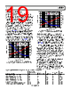
19 / 27 page  Data Sheet ADL5904 Rev. B | Page 19 of 27 CHOOSING A VALUE FOR CRMS CRMS provides the averaging function for the internal rms computation. Using the minimum value for CRMS allows the quickest response time to a pulsed waveform, but leaves signifi- cant output noise on the output voltage signal. However, a large filter capacitor reduces output noise and improves the rms measurement accuracy but at the expense of the response time. In applications where the response time is not critical, place a relatively large capacitor on the CRMS pin. In Figure 44, a value of 100 nF is used. For most signal modulation schemes, this value ensures excellent rms measurement accuracy and low residual output noise. There is no maximum capacitance limit for CRMS. Figure 45 and Figure 46 show how output noise varies with CRMS when the ADL5904 is driven by a single-carrier W-CDMA (Test Model TM1-64, peak envelope power = 10.6 dB, bandwidth = 3.84 MHz) and by an LTE signal (Test Model TM1-20, peak envelope power = 11.58 dB, bandwidth = 20 MHz), respectively. Figure 45 and Figure 46 also show how the value of CRMS affects the response time. This response time is measured by applying an RF burst at 2.14 GHz at 0 dBm to the ADL5904. The 10% to 90% rise time and 90% to 10% fall time are then measured. 0 100 200 300 400 500 600 0.1 1.0 10 100 1k 10k 100k 0.1 1 10 100 1000 CRMS CAPACITANCE (nF) 10% TO 90% RISE TIME (µs) 90% TO 10% FALL TIME (µs) OUTPUT NOISE (mV p-p) Figure 45. Output Noise, Rise and Fall Times vs. CRMS Capacitance, Single-Carrier W-CDMA (Test Model TM1-64) at 900 MHz with PIN = 0 dBm 0 100 200 300 400 600 700 0 0.1 1.0 10 100 1k 500 10k 100k 0.1 1 10 100 1000 CRMS CAPACITANCE (nF) 10% TO 90% RISE TIME (µs) 90% TO 10% FALL TIME (µs) OUTPUT NOISE (mV p-p) Figure 46. Output Noise, Rise and Fall Times vs. CRMS Capacitance, Single-Carrier LTE (Test Model TM1-20) at 900 MHz with PIN = 0 dBm Table 5 shows the recommended minimum values of CRMS for various modulation schemes. Table 5 also shows the output rise and fall times and noise performance. Using lower capacitor values results in faster response times but can result in degraded rms measurement accuracy. If the output noise shown in Table 5 is unacceptably high, it can be reduced by increasing CRMS or by implementing an averaging algorithm after the output voltage of the ADL5904 is sampled by an analog-to-digital converter (ADC). The values in Table 5 were experimentally determined to be the minimum capacitance that ensures good rms accuracy for that particular signal type. This test was initially performed with a large capacitance value on the CRMS pin (for example, 10 µF). The value of VRMS was noted for a fixed input level (for example, −10 dBm). The value of CRMS was then progressively reduced (this can be accomplished with press-down capacitors) until the value of VRMS started to deviate from its original value (this indicates that the accuracy of the rms computation is degrading and that CRMS is becoming too small). In general, the minimum CRMS value required increases as the peak to average ratio of the carrier increases. The minimum required CRMS also tends to increase as the bandwidth of the carrier decreases. With narrow-band carriers, the noise spectrum of the VRMS output tends to have a correspondingly narrow profile. The relatively narrow spectral profile requires a larger value of CRMS that reduces the low-pass corner frequency of the averaging function and ensures a valid rms computation. Table 5. Recommended Minimum CRMS Values for Various Modulation Schemes Modulation/Standard Peak Envelope Power Ratio Ratio (dB) Carrier Bandwidth (MHz) CRMSMIN (nF) Output Noise (mV p-p) Rise/Fall Times (µs) QPSK, 5 MSPS (SQR COS) Filter, α = 0.35) 3.3 5 10 42 4/25 QPSK ,15 MSPS (SQR COS Filter, α = 0.35) 3.3 15 1 38 0.5/6 64 QAM, 1 MSPS (SQR COS Filter, α = 0.35) 7.4 1 100 64 35/276 64 QAM, 5 MSPS (SQR COS Filter, α = 0.35) 7.4 5 100 54 35/276 64 QAM, 13 MSPS (SQR COS Filter, α = 0.35) 7.4 13 10 56 4/25 W-CDMA, One-Carrier, TM1-64 10.6 3.84 100 92 35/276 W-CDMA Four-Carrier, TM1-64, TM1-32, TM1-16, TM1-8 15.96 18.84 100 98 35/276 LTE, TM1, One-Carrier, 20 MHz (2048 QPSK Subcarriers) 11.58 20 100 80 35/276 |
|
|
链接网址 |
| ALLDATASHEET是否为您带来帮助? [ DONATE ] |
关于 Alldatasheet | 广告服务 | 联系我们 | 隐私政策 | 数据表链接 | 链接交换 | 制造商名单 All Rights Reserved©Alldatasheet.com |
| Russian : Alldatasheetru.com | Korean : Alldatasheet.co.kr | Spanish : Alldatasheet.es | French : Alldatasheet.fr | Italian : Alldatasheetit.com Portuguese : Alldatasheetpt.com | Polish : Alldatasheet.pl | Vietnamese : Alldatasheet.vn Indian : Alldatasheet.in | Mexican : Alldatasheet.com.mx | British : Alldatasheet.co.uk | New Zealand : Alldatasheet.co.nz |
|
Family Site : ic2ic.com |
icmetro.com |
 Chinese ▼
 English
 Chinese
 German
 Japanese
 Russian
 Korean
 Spanish
 French
 Italian
 Portuguese
 Polish
 Vietnamese
 Indian
 Mexican
 British
 New Zealand