|
数据搜索系统,热门电子元器件搜索 |
|
|
数据搜索系统,热门电子元器件搜索 |
|
PPC440SPE-RNB533C 数据表(PDF) 55 Page - Applied Micro Circuits Corporation |
|
|
|||||||||||||||||||||||||||||
PPC440SPE-RNB533C 数据表(HTML) 55 Page - Applied Micro Circuits Corporation |
|
|
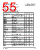
55 / 80 page  PowerPC 440SPe Embedded Processor Revision 1.23 - Sept 21, 2006 AMCC Proprietary 55 Preliminary Data Sheet UART Peripheral Interface UARTSerClk Serial clock input that provides an alternative to the internally generated serial clock. Used in cases where the allowable internally generated clock rates are not satisfactory. I 3.3V LVTTL 1, 4 UART0_Rx UART0 Receive data. I 3.3V LVTTL 1, 4 UART0_Tx UART0 Transmit data. O 3.3V LVTTL 4 UART0_DCD UART0 Data Carrier Detect. I 3.3V LVTTL 6 UART0_DSR UART0 Data Set Ready. I 3.3V LVTTL 6 UART0_CTS UART0 Clear To Send. I 3.3V LVTTL 1, 4, 6 UART0_DTR UART0 Data Terminal Ready. O 3.3V LVTTL 4 UART0_RTS UART0 Request To Send. O 3.3V LVTTL 4 UART0_RI UART0 Ring Indicator. I 3.3V LVTTL w/pull-up 1, 4 UART1_Rx UART1 Receive data. I 3.3V LVTTL 1, 4 UART1_Tx UART1 Transmit data. O 3.3V LVTTL 1, 4 UART1_DSR/CTS UART1 Data Set Ready or Clear To Send. The choice is determined by a DCR register bit setting. I 3.3V LVTTL 1, 4 UART1_DTR/RTS UART1 Request To Send or Data Terminal Ready. The choice is determined by a DCR register bit setting. O 3.3V LVTTL 1, 4 UART2_Rx UART2 Receive data. I 3.3V LVTTL 1, 4 UART2_Tx UART2 Transmit data. O 3.3V LVTTL 1, 4 Interrupts Interface IRQ0:15 External interrupt Requests 0 through 15. These pins are multiplexed with GPIO16:31 I 3.3V LVTTL 1, 5 System Interface Halt Halt from external debugger. I 3.3V LVTTL 1, 4 GPIO00:31 General purpose I/O 0 through 31. The GPIOs are multiplexed with IRQs, and Trace signal IO. Setting is done with the DCR register bits. I/O 3.3V LVTTL SysClk Main system clock input. I 3.3V LVTTL SysErr Set to 1 when a machine check is generated. O 3.3V LVTTL SysPartSel Not used. I NA 3 SysReset Main system reset. External logic can drive this pin low (minimum of 16 cycles) to initiate a system reset. A reset of the PPC440SPe can also be initiated by software. I 3.3V LVTTL 1, 2 ExtReset External Reset. During the PPC440SPe’s reset phase this signal is at down level. O3.3V LVTTL Table 6. Signal Functional Description (Sheet 6 of 8) Notes: 1. Receiver input has hysteresis 2. Must pull up (recommended value is 3k Ω to 3.3V) 3. Must pull down (recommended value is 1k Ω) 4. If not used, must pull up (recommended value is 3k Ω to 3.3V) 5. If not used, must pull down (recommended value is 1k Ω) 6. Strapping input during reset; pull-up or pull-down required Signal Name Description I/O Type Notes |
|
链接网址 |
| ALLDATASHEET是否为您带来帮助? [ DONATE ] |
关于 Alldatasheet | 广告服务 | 联系我们 | 隐私政策 | 数据表链接 | 链接交换 | 制造商名单 All Rights Reserved©Alldatasheet.com |
| Russian : Alldatasheetru.com | Korean : Alldatasheet.co.kr | Spanish : Alldatasheet.es | French : Alldatasheet.fr | Italian : Alldatasheetit.com Portuguese : Alldatasheetpt.com | Polish : Alldatasheet.pl | Vietnamese : Alldatasheet.vn Indian : Alldatasheet.in | Mexican : Alldatasheet.com.mx | British : Alldatasheet.co.uk | New Zealand : Alldatasheet.co.nz |
|
Family Site : ic2ic.com |
icmetro.com |
 Chinese ▼
 English
 Chinese
 German
 Japanese
 Russian
 Korean
 Spanish
 French
 Italian
 Portuguese
 Polish
 Vietnamese
 Indian
 Mexican
 British
 New Zealand