|
数据搜索系统,热门电子元器件搜索 |
|
|
数据搜索系统,热门电子元器件搜索 |
|
PPC405GPR-3JB266Z 数据表(PDF) 33 Page - Applied Micro Circuits Corporation |
|
|
|||||||||||||||||||||||||||||
PPC405GPR-3JB266Z 数据表(HTML) 33 Page - Applied Micro Circuits Corporation |
|
|
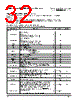
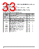
33 / 57 page  405GPr – Power PC 405GPr Embedded Processor AMCC 33 Revision 2.04 – September 7, 2007 Data Sheet PerCS0 Peripheral chip select bank 0. O 5V tolerant 3.3V LVTTL 7 PerCS1:7[GPIO10:16] Seven additional peripheral chip selects or General Purpose I/O. To access this function, software must toggle a DCR bit. O[I/O] 5V tolerant 3.3V LVTTL 1, 7 PerOE Used by either the peripheral controller or the DMA controller depending upon the type of transfer involved. When the PPC405GPr is the bus master, it enables the selected device to drive the bus. O 5V tolerant 3.3V LVTTL 7 PerR/W Used by the PPC405GPr when not in external master mode, as output by either the peripheral controller or DMA controller depending upon the type of transfer involved. High indicates a read from memory, low indicates a write to memory. Otherwise it used by the external master as an input to indicate the direction of data transfer. I/O 5V tolerant 3.3V LVTTL 1 PerReady Used by a peripheral slave to indicate it is ready to transfer data. I 5V tolerant 3.3V LVTTL 1 PerBLast Used by the PPC405GPr when not in external master mode, otherwise used by external master. Indicates the last transfer of a memory access. I/O 5V tolerant 3.3V LVTTL 1, 7 DMAReq0:3 DMAReq0:3 are used by slave peripherals to indicate they are prepared to transfer data. I 5V tolerant 3.3V LVTTL 1 DMAAck0:3 DMAAck0:3 are used by the PPC405GPr to cause the DMA peripheral to transfer data. O 5V tolerant 3.3V LVTTL 6 EOT0:3/TC0:3 End Of Transfer/Terminal Count. I/O 5V tolerant 3.3V LVTTL 1 Signal Functional Description (Sheet 4 of 8) Multiplexed signals are shown in brackets following the first signal name assigned to each multiplexed ball. Notes: 1. Receiver input has hysteresis. 2. Must pull up. See “Pull-Up and Pull-Down Resistors” on page 29 for recommended termination values. 3. Must pull down. See “Pull-Up and Pull-Down Resistors” on page 29 for recommended termination values. 4. If not used, must pull up. 5. If not used, must pull down. 6. Strapping input during reset; pull up or pull down as required. 7. Pull-up may be required. See “External Bus Control Signals” on page 29. Signal Name Description I/O Type Notes |
|
链接网址 |
| ALLDATASHEET是否为您带来帮助? [ DONATE ] |
关于 Alldatasheet | 广告服务 | 联系我们 | 隐私政策 | 数据表链接 | 链接交换 | 制造商名单 All Rights Reserved©Alldatasheet.com |
| Russian : Alldatasheetru.com | Korean : Alldatasheet.co.kr | Spanish : Alldatasheet.es | French : Alldatasheet.fr | Italian : Alldatasheetit.com Portuguese : Alldatasheetpt.com | Polish : Alldatasheet.pl | Vietnamese : Alldatasheet.vn Indian : Alldatasheet.in | Mexican : Alldatasheet.com.mx | British : Alldatasheet.co.uk | New Zealand : Alldatasheet.co.nz |
|
Family Site : ic2ic.com |
icmetro.com |
 Chinese ▼
 English
 Chinese
 German
 Japanese
 Russian
 Korean
 Spanish
 French
 Italian
 Portuguese
 Polish
 Vietnamese
 Indian
 Mexican
 British
 New Zealand