|
数据搜索系统,热门电子元器件搜索 |
|
|
数据搜索系统,热门电子元器件搜索 |
|
EVLSTDRIVEG611 数据表(PDF) 6 Page - STMicroelectronics |
|
|
|||||||||||||||||||||||||||||
EVLSTDRIVEG611 数据表(HTML) 6 Page - STMicroelectronics |
|
|
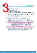
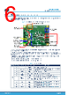
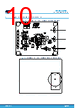
6 / 16 page  3 Board power-up and input connection The following image shows how to supply the EVLSTDRIVEG611, how to provide LIN and HIN inputs and set the programmable deadtime generator. Figure 3. EVLSTDRIVEG611 - supply and signal connection VCC GND J1: HV BUS J2: OUT, Half-bridge middle point J3: POWER GROUND Single signal input for deadtime generator TR1: High-side deadtime generator TR2: Low-side deadtime generator Direct LIN & HIN inputs (see Table 2) J5: 12V typ gate driver supply J4: Driver supply and inputs connector J1 & J3: Half bridge high voltage supply + _ Direct LIN & HIN inputs selector Single PWM input selector The LIN, HIN inputs can be provided from the onboard deadtime generator or directly from an external generator or control device (such as DSP/MCU). The deadtime value set by the onboard deadtime generator, fed by PWM input signal on J4, can be tuned by setting TR1 and TR2. The typical deadtime value with the trimmer in the default manufacturing middle position is about 700 ns. It is possible to change the deadtime generator range by changing C21 and C23. Polarity of PWM input can be modified with R27 and R28 as in Table 3. TR2 sets the deadtime between high-side turn-off and low-side turn-on. TR1 sets the deadtime between low-side turn-off and high-side turn-on. Table 1. Connector map Ref Pin # Name Function Description J4 1 VCC IN power Board supply voltage (12 V typ.) 2 VDD (3V3) OUT power Output voltage of onboard 3.3 V (adj.) regulator: it can be used to supply external circuitry (up to about 50 mA) 3 STBY IN digital Standby input signal (active low) 4 CIN OUT analog Low-side current sense resistor voltage 6 FLT OUT digital Fault output (overcurrent, UVLO, overtemperature) 7 SD/OD IN digital / OUT analog Disable input signal (0 to 3.3 V or up to 20 V) – see Table 3. Open-drain output to set the disable time after an overcurrent event (default ~1 ms). 9 HIN IN digital HIN direct input signal (0 to 3.3 V or up to 20 V): mount R23 and remove R25 – see Table 2 and Table 3 10 LIN IN digital LIN direct input signal (0 to 3.3 V or up to 20 V): mount R29 and remove R31 – see Table 2 and Table 3 12 PWM IN digital PWM input signal (0 to 3.3 V or 5 V) – see Table 2 and Table 3 EVLSTDRIVEG611 Board power-up and input connection DB5115 - Rev 1 page 6/16 |
|
|
链接网址 |
| ALLDATASHEET是否为您带来帮助? [ DONATE ] |
关于 Alldatasheet | 广告服务 | 联系我们 | 隐私政策 | 数据表链接 | 链接交换 | 制造商名单 All Rights Reserved©Alldatasheet.com |
| Russian : Alldatasheetru.com | Korean : Alldatasheet.co.kr | Spanish : Alldatasheet.es | French : Alldatasheet.fr | Italian : Alldatasheetit.com Portuguese : Alldatasheetpt.com | Polish : Alldatasheet.pl | Vietnamese : Alldatasheet.vn Indian : Alldatasheet.in | Mexican : Alldatasheet.com.mx | British : Alldatasheet.co.uk | New Zealand : Alldatasheet.co.nz |
|
Family Site : ic2ic.com |
icmetro.com |
 Chinese ▼
 English
 Chinese
 German
 Japanese
 Russian
 Korean
 Spanish
 French
 Italian
 Portuguese
 Polish
 Vietnamese
 Indian
 Mexican
 British
 New Zealand