|
数据搜索系统,热门电子元器件搜索 |
|
|
数据搜索系统,热门电子元器件搜索 |
|
EVLSTDRIVEG611 数据表(PDF) 7 Page - STMicroelectronics |
|
|
|||||||||||||||||||||||||||||
EVLSTDRIVEG611 数据表(HTML) 7 Page - STMicroelectronics |
|
|
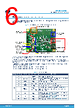
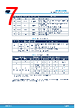
7 / 16 page  Ref Pin # Name Function Description J4 5, 8, 11 GND Power Board reference potential J2 1, 2, 3 OUT OUT power These three pins are connected to the OUT pin of the power stage: connect the load to this terminal J1 1, 2, 3 HV IN power These three pins are connected to the high voltage (HV) of the GaN power stage. Connect the half-bridge high-voltage positive supply. J3 1, 2, 3 GND_P Power These three pins are connected to power ground. Connect the half-bridge high-voltage negative supply. J5 1 VCC IN power Board driver supply voltage 12 V typ. (as J4 pin 1) 2 GND Power Board reference potential Table 2. Device input selection Board status Input source R25, R31 R23, R29 Function and description Default PWM J4: pin 12 0 Ω (closed) Open LIN & HIN are generated by the onboard deadtime generator from a single PWM signal. PWM input range: 0 to 3.3 V (5 V compatible) PWM J4: pin 9, 10 Open 0 Ω (closed) Direct connection to LIN and HIN STDRIVEG611 pins. LIN, HIN input range: up to 20 V Table 3. Input signal truth table Board inputs PWM polarity Driver inputs and outputs (1) STBY SD/OD PWM R27, R28 LIN HIN Low-side High-side Half-bridge output L X X X X X Off Off High-Z X L H (default, pull-up) H (default, pull-up) L R27 open, R28 closed (default) H L On Off GND H L H Off On (2) HV (2) L R27 closed, R28 open L H Off On (2) HV (2) H H L On Off GND 1. With device not in VCC and VCCL UVLO, CIN < CINth and not in overtemperature. 2. With device not in VCCH UVLO The recommended power-on sequence is to turn VCC on first, then apply the HV bus voltage. The recommended power-off sequence is to turn off the HV bus supply first, then VCC. EVLSTDRIVEG611 Board power-up and input connection DB5115 - Rev 1 page 7/16 |
|
|
链接网址 |
| ALLDATASHEET是否为您带来帮助? [ DONATE ] |
关于 Alldatasheet | 广告服务 | 联系我们 | 隐私政策 | 数据表链接 | 链接交换 | 制造商名单 All Rights Reserved©Alldatasheet.com |
| Russian : Alldatasheetru.com | Korean : Alldatasheet.co.kr | Spanish : Alldatasheet.es | French : Alldatasheet.fr | Italian : Alldatasheetit.com Portuguese : Alldatasheetpt.com | Polish : Alldatasheet.pl | Vietnamese : Alldatasheet.vn Indian : Alldatasheet.in | Mexican : Alldatasheet.com.mx | British : Alldatasheet.co.uk | New Zealand : Alldatasheet.co.nz |
|
Family Site : ic2ic.com |
icmetro.com |
 Chinese ▼
 English
 Chinese
 German
 Japanese
 Russian
 Korean
 Spanish
 French
 Italian
 Portuguese
 Polish
 Vietnamese
 Indian
 Mexican
 British
 New Zealand