|
数据搜索系统,热门电子元器件搜索 |
|
|
数据搜索系统,热门电子元器件搜索 |
|
STDRIVE101TR 数据表(PDF) 15 Page - STMicroelectronics |
|
|
|||||||||||||||||||||||||||||
STDRIVE101TR 数据表(HTML) 15 Page - STMicroelectronics |
|
|
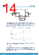
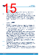
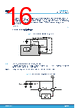
15 / 32 page  Equation 2 (2) PREG12= VS−VREG12 ⋅IREG12 where VS is the voltage supply of the STDRIVE101, VREG12 is the regulator output voltage and IREG12 is the average current consumption described previously. Note: The size of the external power MOSFETs and the switching frequency increase the gate driver’s consumption, thus reducing the current availability for external loads. In addition to the average value IREG12 dynamic contributions must be considered: these are the currents needed to charge the bootstrap capacitors, e.g. after the high-side MOSFET is kept on for a considerable amount of time or after leaving the stand-by condition. In these cases, the amount of current is higher than IREG12lim, so it is mainly provided by the bypass capacitor CREG12 connected to REG12 pin. In this situation, a voltage drop ΔVREG12 occurs on REG12, while the LDO maximum current IREG12lim mainly recharges CREG12. During this recharge time (tcharge,REG12 expressed in Equation 3), the availability of current for external loads is reduced. Equation 3 (3) tcℎarge,REG12>CREG∆VREG12 IREG12lim 5.2.1 Bootstrap section The bootstrap circuitry allows to generate a voltage higher than the supply VS and it is used to supply the high- side drivers. When one high-side MOSFET is turned on, its source voltage (OUTx pin) increases up to VS. Therefore, the gate must be driven at a voltage higher than VS. The bootstrap capacitor is referred to the OUTx pin: • When the OUTx pin is forced to GND (i.e. the respective low-side MOSFET is on), the bootstrap capacitor is charged through the bootstrap diode. • When the OUTx is forced to VS (i.e. the respective high-side MOSFET is on), the bootstrap capacitor supplies the respective high-side driver and discharges. The voltage drop on the bootstrap capacitors corresponds to the supply of the high-side drivers. Each bootstrap capacitor must be charged after the corresponding high-side is turned on, otherwise its voltage falls below the VBO(On) - VBO(Hyst) threshold, causing the turning off of the respective driver ( Section 5.5 ). A limitation in a bootstrap architecture is that the high-side MOSFET cannot be kept on for an indefinite amount of time. In fact, when the high-side is on, the respective bootstrap capacitor starts discharging. If not recharged, the bootstrap capacitor voltage falls below the VBO(On) - VBO(Hyst) (i.e. the UVLO on BOOTx pin). For this reason, working at 100% duty cycle is possible, but only for a limited number of PWM periods. The bigger the bootstrap capacitor, the longer the time the high-side MOSFET can be kept on. To avoid excessive drop on the REG12 pin, a proper bypass capacitor is required. Even using an external supply connected to the REG12 pin, it is important to have a bypass capacitor with low ESR providing fast current transients when required by the bootstrap capacitors. The bypass capacitor on REG12 pin must provide the charge for the three bootstrap capacitors: the bigger the bootstrap capacitors are, the bigger should be the REG12 capacitor (refer to Equation 4 in Section 5.2.1.2 ). 5.2.1.1 Power-up and wake-up During the power-up or after leaving the standby condition, there may be no charge in bootstrap capacitors. In these cases, the drivers cannot start immediately with normal operation, but the bootstrap capacitor should be charged turning on the low-side MOSFET. At the beginning of this procedure, a large amount of current could be required. If the internal 12 V LDO regulator is used, its current is limited at IREG12lim (Section 5.2 ). 5.2.1.2 Charging time and external bootstrap diodes The charging time required to charge the bootstrap capacitors depends on their value but also on the resistance of the bootstrap diode (RDS_diode), which limits the current flow. In order to reduce the minimum time for bootstrap recharge (i.e. the minimum time the low-side MOSFET must be on), external bootstrap diodes can be used as shown in Figure 11. STDRIVE101 12 V LDO linear regulator DS13472 - Rev 1 page 15/32 |
|
链接网址 |
| ALLDATASHEET是否为您带来帮助? [ DONATE ] |
关于 Alldatasheet | 广告服务 | 联系我们 | 隐私政策 | 数据表链接 | 链接交换 | 制造商名单 All Rights Reserved©Alldatasheet.com |
| Russian : Alldatasheetru.com | Korean : Alldatasheet.co.kr | Spanish : Alldatasheet.es | French : Alldatasheet.fr | Italian : Alldatasheetit.com Portuguese : Alldatasheetpt.com | Polish : Alldatasheet.pl | Vietnamese : Alldatasheet.vn Indian : Alldatasheet.in | Mexican : Alldatasheet.com.mx | British : Alldatasheet.co.uk | New Zealand : Alldatasheet.co.nz |
|
Family Site : ic2ic.com |
icmetro.com |
 Chinese ▼
 English
 Chinese
 German
 Japanese
 Russian
 Korean
 Spanish
 French
 Italian
 Portuguese
 Polish
 Vietnamese
 Indian
 Mexican
 British
 New Zealand