|
数据搜索系统,热门电子元器件搜索 |
|
|
数据搜索系统,热门电子元器件搜索 |
|
STDRIVE101TR 数据表(PDF) 31 Page - STMicroelectronics |
|
|
|||||||||||||||||||||||||||||
STDRIVE101TR 数据表(HTML) 31 Page - STMicroelectronics |
|
|
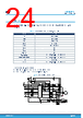
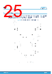
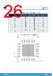
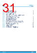
31 / 32 page  List of figures Figure 1. STDRIVE101 block diagram........................................................... 2 Figure 2. INx timings and deadtime (ENx/INx mode) ................................................. 9 Figure 3. ENx timings (ENx/INx mode) .......................................................... 9 Figure 4. INHx and INLx timings (INHx/INLx mode)................................................. 10 Figure 5. Overcurrent comparator timings ....................................................... 10 Figure 6. VDS monitoring protection timing ....................................................... 10 Figure 7. STDRIVE101 pin connection in QFN 4x4 24L with exposed PAD (Top view) ......................... 11 Figure 8. Gate drivers’ outputs characteristics in UVLO conditions ...................................... 13 Figure 9. 12 V LDO linear regulator typical configuration ............................................. 14 Figure 10. Typical current consumption (driver’ outputs unloaded) ....................................... 14 Figure 11. External bootstrap diode configuration ................................................... 16 Figure 12. 12 V LDO supply voltage externally provided .............................................. 16 Figure 13. Deadtime management for short pulses .................................................. 18 Figure 14. Typical deadtime vs. DT resistor value ................................................... 18 Figure 15. Standby and wake-up time (ENx/INx mode, with VS = VREG12 = 12 V) ............................. 19 Figure 16. Standby and wake-up time (INHx/INLx mode, with VS = VREG12 = 12 V) ........................... 19 Figure 17. Power-up sequence, internal 12 V regulator used ........................................... 20 Figure 18. Power-up sequence, external supply on REG12 pin ......................................... 21 Figure 19. Thermal shutdown management ....................................................... 22 Figure 20. ESD protection strategy ............................................................. 23 Figure 21. Typical application schematic ......................................................... 24 Figure 22. VFQFPN 4x4x1.0 24 PITCH 0.5 package outline ........................................... 25 Figure 23. VFQFPN 4x4x1.0 24 PITCH 0.5 suggested footprint ......................................... 26 STDRIVE101 List of figures DS13472 - Rev 1 page 31/32 |
|
链接网址 |
| ALLDATASHEET是否为您带来帮助? [ DONATE ] |
关于 Alldatasheet | 广告服务 | 联系我们 | 隐私政策 | 数据表链接 | 链接交换 | 制造商名单 All Rights Reserved©Alldatasheet.com |
| Russian : Alldatasheetru.com | Korean : Alldatasheet.co.kr | Spanish : Alldatasheet.es | French : Alldatasheet.fr | Italian : Alldatasheetit.com Portuguese : Alldatasheetpt.com | Polish : Alldatasheet.pl | Vietnamese : Alldatasheet.vn Indian : Alldatasheet.in | Mexican : Alldatasheet.com.mx | British : Alldatasheet.co.uk | New Zealand : Alldatasheet.co.nz |
|
Family Site : ic2ic.com |
icmetro.com |
 Chinese ▼
 English
 Chinese
 German
 Japanese
 Russian
 Korean
 Spanish
 French
 Italian
 Portuguese
 Polish
 Vietnamese
 Indian
 Mexican
 British
 New Zealand