|
数据搜索系统,热门电子元器件搜索 |
|
|
数据搜索系统,热门电子元器件搜索 |
|
R5F10DMDCLFB 数据表(PDF) 113 Page - Renesas Technology Corp |
|
|
|||||||||||||||||||||||||||||
R5F10DMDCLFB 数据表(HTML) 113 Page - Renesas Technology Corp |
|
|
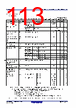
113 / 139 page  RL78/D1A 4. ELECTRICAL SPECIFICATIONS (L GRADE PRODUCT) R01DS0463EJ0120 Rev. 1.20 Page 113 of 135 Mar 31, 2026 4.5 AC characteristics 4.5.1 Basic operation TA = -40 to +105 °C, 2.7 V ≤ = EVDD0 = EVDD1 ≤ VDD = SMVDD0 = SMVDD1 ≤ 5.5 V, VSS = EVSS0 = EVSS1 = SMVSS0 = SMVSS1 = 0 V Parameter Symbols Conditions Min. Typ. Max. Unit Instruction cycle (minimum instruction execution time) TCY Main system clock operation (Including PLL) High speed main run 0.04166 Note 1 1 μs Sub system clock operation SDIV = 0 1/fXT (Typ. 30.5) μs External main system clock frequency fEX Square wave input to EXCLK 2 20 MHz External main system clock (square wave) input high/low level width tEXH tEXL Square wave input to EXCLK 24 ns Timer input high/low level width tTIH tTIL TI00 to TI07, TI10 to TI17, TI20 to TI27 1/fMCK+10 Note 2 ns Port output frequency fGPO P80 to P87, P90 to P97 C = 30 pF 4.0 V ≤ SMVDD 2 MHz P20 to P27, P150 to P152 C = 30 pF 4.0 V ≤ VDD 2 MHz P73,P135 C = 30 pF 4.0 V ≤ EVDD 8 MHz Other than the above C = 30 pF 4.0 V ≤ EVDD 16 MHz 2.7 V ≤ EVDD < 4.0 V 8 MHz External interrupt input high/low level width Note 3 tINTH tINTL INTP0 to INTP5, INTPLR0, INTPLR1 1 μs RESET ____________ input low level width Note 3 tRSL RESET ____________ 10 μs Analog noise filter rejection pulse width Note 4 tWRJ INTP0 to INTP5, INTPLR0, INTPLR1, ADTRG 30 50 1000 ns ADTRG input high level width tATH Without noise filter AWC=0 1/fCLK+10 ns AWC=1 10 ns With noise filter AWC=0 1/fCLK+10 or tWRJ (Note 5) ns AWC=1 tWRJ (Note 5) ns Notes 1. Value is in case of fCLK is 24.0 MHz. It is also allowed to exceed frequency up to +3%. 2. fMCK shows the frequency value of operation clock for TAU. Usually, fMCK is defined by MHz but this specification is defined by ns. It is not defined by µs, so please be careful. 3. Pulses longer than this value will pass the input filter. 4. Pulses shorter than this value do not pass the input filters. 5. If the value of “1/fCLK+10 [ns]” is less than tWRJ, please use tWRJ value instead of “1/fCLK +10 [ns]”. Caution Different voltage between EVDD and VDD is allowed only when LCDM register is initial value. <R> |
|
链接网址 |
| ALLDATASHEET是否为您带来帮助? [ DONATE ] |
关于 Alldatasheet | 广告服务 | 联系我们 | 隐私政策 | 数据表链接 | 链接交换 | 制造商名单 All Rights Reserved©Alldatasheet.com |
| Russian : Alldatasheetru.com | Korean : Alldatasheet.co.kr | Spanish : Alldatasheet.es | French : Alldatasheet.fr | Italian : Alldatasheetit.com Portuguese : Alldatasheetpt.com | Polish : Alldatasheet.pl | Vietnamese : Alldatasheet.vn Indian : Alldatasheet.in | Mexican : Alldatasheet.com.mx | British : Alldatasheet.co.uk | New Zealand : Alldatasheet.co.nz |
|
Family Site : ic2ic.com |
icmetro.com |
 Chinese ▼
 English
 Chinese
 German
 Japanese
 Russian
 Korean
 Spanish
 French
 Italian
 Portuguese
 Polish
 Vietnamese
 Indian
 Mexican
 British
 New Zealand