|
数据搜索系统,热门电子元器件搜索 |
|
|
数据搜索系统,热门电子元器件搜索 |
|
ADP1613ARMZ-R7 数据表(PDF) 16 Page - Analog Devices |
|
|
|||||||||||||||||||||||||||||
ADP1613ARMZ-R7 数据表(HTML) 16 Page - Analog Devices |
|
|
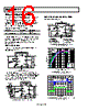
16 / 28 page  ADP1612/ADP1613 Rev. A | Page 16 of 28 TYPICAL APPLICATION CIRCUITS Both the ADP1612 and ADP1613 can be used in the application circuits in this section. The ADP1612 is geared toward applications requiring input voltages as low as 1.8 V, where the ADP1613 is more suited for applications needing the output power capabilities of a 2.0 A switch. The primary differences are shown in Table 6. Table 6. ADP1612/ADP1613 Differences Parameter ADP1612 ADP1613 Current Limit 1.4 A 2.0 A Input Voltage Range 1.8 V to 5.5 V 2.5 V to 5.5 V The Step-Up Regulator Circuit Examples section recommends component values for several common input, output, and load conditions. The equations in the Applications Information section can be used to select components for alternate configurations. STEP-UP REGULATOR The circuit in Figure 36 shows the ADP1612/ADP1613 in a basic step-up configuration. ADP1612/ ADP1613 6 3 7 8 5 2 1 4 VIN EN FREQ SS SW FB COMP GND ON OFF 1.3MHz 650kHz (DEFAULT) VOUT VIN L1 CIN CSS COUT CCOMP RCOMP R1 R2 D1 Figure 36. Step-Up Regulator The modified step-up circuit in Figure 37 incorporates true shutdown capability advantageous for battery-powered applica- tions requiring low standby current. Driving the EN pin below 0.3 V shuts down the ADP1612/ADP1613 and completely disconnects the input from the output. ADP1612/ ADP1613 6 3 7 8 5 2 1 4 VIN EN FREQ SS SW FB COMP GND 1.3MHz 650kHz (DEFAULT) VOUT L1 CIN CSS COUT CCOMP RCOMP R1 R2 D1 VIN R3 10k Ω NTGD1100L Q1 A B Q1 ON OFF Figure 37. Step-Up Regulator with True Shutdown STEP-UP REGULATOR CIRCUIT EXAMPLES ADP1612 Step-Up Regulator ADP1612 6 3 7 8 5 2 1 4 VIN EN FREQ SS SW FB COMP GND ON OFF VOUT = 5V VIN = 1.8V TO 4.2V L1 4.7µH CSS 33nF COUT 10µF CCOMP 3300pF RCOMP 6.8k Ω R1 30k Ω R2 10k Ω D1 3A, 40V CIN 10µF L1: DO3316P-472ML D1: MBRA340T3G R1: RC0805FR-0730KL R2: CRCW080510K0FKEA RCOMP: RC0805JR-076K8L CCOMP: ECJ-2VB1H332K CIN: GRM21BR61C106KE15L COUT: GRM32DR71E106KA12L CSS: ECJ-2VB1H333K Figure 38. ADP1612 Step-Up Regulator Configuration VOUT = 5 V, fSW = 650 kHz 100 90 80 70 60 50 40 30 1 10 100 1k 10k LOAD CURRENT (mA) VOUT = 5V fSW = 650kHz TA = 25°C VIN = 1.8V VIN = 2.7V VIN = 3.3V VIN = 4.2V ADP1612 Figure 39. ADP1612 Efficiency vs. Load Current VOUT = 5 V, fSW = 650 kHz VOUT = 5V fSW = 650kHz T TIME (100µs/DIV) OUTPUT VOLTAGE (50mV/DIV) AC-COUPLED LOAD CURRENT (50mA/DIV) Figure 40. ADP1612 50 mA to 150 mA Load Transient (VIN = 3.3 V) VOUT = 5 V, fSW = 650 kHz |
|
|
链接网址 |
| ALLDATASHEET是否为您带来帮助? [ DONATE ] |
关于 Alldatasheet | 广告服务 | 联系我们 | 隐私政策 | 数据表链接 | 链接交换 | 制造商名单 All Rights Reserved©Alldatasheet.com |
| Russian : Alldatasheetru.com | Korean : Alldatasheet.co.kr | Spanish : Alldatasheet.es | French : Alldatasheet.fr | Italian : Alldatasheetit.com Portuguese : Alldatasheetpt.com | Polish : Alldatasheet.pl | Vietnamese : Alldatasheet.vn Indian : Alldatasheet.in | Mexican : Alldatasheet.com.mx | British : Alldatasheet.co.uk | New Zealand : Alldatasheet.co.nz |
|
Family Site : ic2ic.com |
icmetro.com |
 Chinese ▼
 English
 Chinese
 German
 Japanese
 Russian
 Korean
 Spanish
 French
 Italian
 Portuguese
 Polish
 Vietnamese
 Indian
 Mexican
 British
 New Zealand