|
数据搜索系统,热门电子元器件搜索 |
|
|
数据搜索系统,热门电子元器件搜索 |
|
AD8142ACPZ-R2 数据表(PDF) 17 Page - Analog Devices |
|
|
|||||||||||||||||||||||||||||
AD8142ACPZ-R2 数据表(HTML) 17 Page - Analog Devices |
|
|
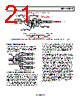
17 / 24 page  AD8141/AD8142 Rev. 0 | Page 17 of 24 The desired differential output in this example is 1.4 V p-p because the terminated input signal is 0.7 V p-p and the closed- loop gain = 2. The actual differential output voltage is equal to (0.725 V p-p)(2 kΩ/1038.3 Ω) = 1.4 V p-p. This illustrates how the two aforementioned effects cancel for large RF and RG. AD8142 SYNC-ON-COMMON-MODE The AD8142 includes on-chip, sync-on-common-mode circuitry that encodes externally applied HSYNC and VSYNC signals onto the common-mode output voltages of each of the R, G, and B drivers. The circuit encodes the horizontal and vertical sync pulses in a way that results in low radiated energy. A simplified circuit that illustrates how the pulses are encoded is shown in Figure 41. For a more detailed description of the sync scheme, see the Applications Information section. DRIVING A CAPACITIVE LOAD A purely capacitive load can react with the output impedance of the drivers to reduce phase margin, resulting in high frequency ringing in the pulse response. The best way to minimize this effect is to place the source termination resistors immediately at the amplifier outputs to minimize parasitic capacitances formed by unnecessarily long traces. The sync-on-common-mode circuit generates a current based on the voltage applied to the SYNC LEVEL input pin (Pin 18) with respect to the negative supply. With SYNC LEVEL input tied to VS−, the common-mode output of all drivers is set at 1.5 V above the negative supply. Using a resistor divider, a voltage can be applied between VS− and SYNC LEVEL that determines the maximum deviation of the common-mode outputs from their midsupply level. If, for instance, SYNC LEVEL − VS− = 0.5 V and the supply voltage is 5 V, then the common-mode outputs fall within an envelope of 1.5 V ± 0.5 V. The state of each VOUT, cm output based on the HSYNC and VSYNC inputs is determined by the equations defined in the Applications Information section. DISABLE The AD8141 and AD8142 have disable pins that, when pulled high, significantly reduce the power consumed while simultaneously placing the outputs in high-Z states. The disable feature can be used to multiplex two drivers. See Figure 17, Figure 19, and Figure 22 for the disabled input-to-output isolation, output impedance, and response performance. The threshold levels for the disable pin are listed in Table 1. An output glitch occurs whenever the disable feature is asserted or deasserted. See the Applications Information section for details. For the positive supplies between 2.5 V and 5 V, the sync-on- common-mode circuit can be used by directly applying standard HSYNC and VSYNC signals to the respective AD8142 inputs. These inputs adhere to standard logic thresholds (see Table 1 for the exact levels). The HSYNC and VSYNC inputs, therefore, can be driven directly off the output of a computer video card without concern of being overdriven. The input path from the HSYNC and VSYNC inputs to the switches in the current mode level-shifting circuit are well matched to eliminate false switching transients. This maximizes common-mode balance and minimizes radiated energy. H V V H HR R R R R R H V VS– BLUE VOCM SYNC LEVEL HSYNC VSYNC VS+ H V H R V MIRROR MIRROR V V V RED VOCM GREEN VOCM Figure 41. Sync-On-Common-Mode Simplified Circuit |
|
|
链接网址 |
| ALLDATASHEET是否为您带来帮助? [ DONATE ] |
关于 Alldatasheet | 广告服务 | 联系我们 | 隐私政策 | 数据表链接 | 链接交换 | 制造商名单 All Rights Reserved©Alldatasheet.com |
| Russian : Alldatasheetru.com | Korean : Alldatasheet.co.kr | Spanish : Alldatasheet.es | French : Alldatasheet.fr | Italian : Alldatasheetit.com Portuguese : Alldatasheetpt.com | Polish : Alldatasheet.pl | Vietnamese : Alldatasheet.vn Indian : Alldatasheet.in | Mexican : Alldatasheet.com.mx | British : Alldatasheet.co.uk | New Zealand : Alldatasheet.co.nz |
|
Family Site : ic2ic.com |
icmetro.com |
 Chinese ▼
 English
 Chinese
 German
 Japanese
 Russian
 Korean
 Spanish
 French
 Italian
 Portuguese
 Polish
 Vietnamese
 Indian
 Mexican
 British
 New Zealand