|
数据搜索系统,热门电子元器件搜索 |
|
|
数据搜索系统,热门电子元器件搜索 |
|
AD8420ARMZ-R7 数据表(PDF) 19 Page - Analog Devices |
|
|
|||||||||||||||||||||||||||||
AD8420ARMZ-R7 数据表(HTML) 19 Page - Analog Devices |
|
|
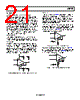
19 / 28 page  Data Sheet AD8420 Rev. 0 | Page 19 of 28 THEORY OF OPERATION +IN –IN gm1 I2 I1 I3 +VS –VS +VS –VS +VS –VS R2 R1 VOUT FB REF AD8420 gm2 ESD PROTECTION A Vb ESD PROTECTION Figure 58. Simplified Schematic ARCHITECTURE The AD8420 is based on an indirect current feedback topology consisting of three amplifiers: two matched transconductance amplifiers that convert voltage to current and one integrator amplifier that converts current to voltage. For the AD8420, assume that all initial voltages and currents are zero until a positive differential voltage is applied between the inputs, +IN and −IN. Transconductance Amplifier gm1 converts this input voltage into a current, I1. Because the voltage across gm2 is initially zero, I2 is zero and I3 equals I1. I3 is integrated to the output, making the output voltage, VOUT, increase. This voltage continues to increase until the same differ- ential input voltage across the inputs of gm1 is replicated across the inputs of gm2, generating a current (I2) equal to I1. This reduces the Difference Current I3 to zero so that the output remains at a stable voltage. The gain in the configuration shown in Figure 58 is set by R2 and R1. In traditional instrumentation amplifiers, the input common- mode voltage can limit the available output swing, typically depicted in a hexagon plot. Because the AD8420 converts the input differential signals to current, this limit does not apply. This is particularly important when amplifying a signal with a common- mode voltage near one of the supply rails. To improve robustness and ease of use, the AD8420 includes overvoltage protection on its inputs. This protection scheme allows wide differential input voltages without damaging the part. SETTING THE GAIN The transfer function of the AD8420 is VOUT = G(V+IN − V−IN) + VREF where: R1 R2 G + =1 Table 7. Suggested Resistors for Various Gains, 1% Resistors R1 (kΩ) R2 (kΩ) Gain None Short 1.00 49.9 49.9 2.00 20 80.6 5.03 10 90.9 10.09 5 95.3 20.06 2 97.6 49.8 1 100 101 1 200 201 1 499 500 1 1000 1001 While the ratio of R2 to R1 sets the gain, the designer determines the absolute value of the resistors. Larger values reduce power consumption and output loading; smaller values limit the FB input bias current and offset current error. For best output swing and distortion performance, keep (R1 + R2) || RL ≥ 20 kΩ. A method that allows large value feedback resistors while limiting FB bias current error is to place a resistor of value R1 || R2 in series with the REF terminal, as shown in Figure 59. At higher gains, this resistor can simply be the same value as R1. AD8420 +IN –IN REF FB VOUT G = 1 + R2 R1 IB+ IB– VREF R1 R2 R1 ||R2 + – IBR IBF Figure 59. Cancelling Out Error from FB Input Bias Current |
|
|
链接网址 |
| ALLDATASHEET是否为您带来帮助? [ DONATE ] |
关于 Alldatasheet | 广告服务 | 联系我们 | 隐私政策 | 数据表链接 | 链接交换 | 制造商名单 All Rights Reserved©Alldatasheet.com |
| Russian : Alldatasheetru.com | Korean : Alldatasheet.co.kr | Spanish : Alldatasheet.es | French : Alldatasheet.fr | Italian : Alldatasheetit.com Portuguese : Alldatasheetpt.com | Polish : Alldatasheet.pl | Vietnamese : Alldatasheet.vn Indian : Alldatasheet.in | Mexican : Alldatasheet.com.mx | British : Alldatasheet.co.uk | New Zealand : Alldatasheet.co.nz |
|
Family Site : ic2ic.com |
icmetro.com |
 Chinese ▼
 English
 Chinese
 German
 Japanese
 Russian
 Korean
 Spanish
 French
 Italian
 Portuguese
 Polish
 Vietnamese
 Indian
 Mexican
 British
 New Zealand