|
数据搜索系统,热门电子元器件搜索 |
|
|
数据搜索系统,热门电子元器件搜索 |
|
AD8420ARMZ-R7 数据表(PDF) 20 Page - Analog Devices |
|
|
|||||||||||||||||||||||||||||
AD8420ARMZ-R7 数据表(HTML) 20 Page - Analog Devices |
|
|
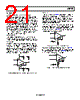
20 / 28 page  AD8420 Data Sheet Rev. 0 | Page 20 of 28 GAIN ACCURACY Unlike most instrumentation amplifiers, the relative match of the two gain setting resistors determines the gain accuracy of the AD8420 rather than a single resistor. For example, if two resistors have exactly the same absolute error, there is no error in gain. Conversely, two 1% resistors can cause approximately 2% maximum gain error at high gains. Temperature coefficient mismatch of the gain setting resistors increases the gain drift of the instrumentation amplifier circuit. Because these external resistors do not have to match any on-chip resistors, resistors with good TC tracking can achieve excellent gain drift. When the differential voltage at the inputs approaches the differential input limit, the diodes start to conduct, limiting the voltage seen by the inputs. This can look like increased gain error at large differential inputs. Performance of the AD8420 is specified for ±1 V differential from −40°C to +85°C. However, at higher temperatures, the reduced forward voltage of the diodes limits the differential input to a smaller voltage. Figure 60 tracks 1% error across the operating temperature range to show the effect of temperature on the input limit. –40 –25 –10 5 20 35 50 65 80 95 110 125 TEMPERATURE (°C) 0 2.0 1.8 1.6 1.4 1.2 1.0 0.8 0.6 0.4 0.2 POSITIVE VOLTAGE NEGATIVE VOLTAGE VS = ±15V Figure 60. Differential Input Limit vs. Temperature INPUT VOLTAGE RANGE The allowed input range of the AD8420 is much simpler than traditional architectures. For the transfer function of the AD8420 to be valid, the input voltage should follow two rules: • Keep the differential input voltage within ±1 V. • Keep the voltage on the +IN, −IN, REF, and FB pins in the specified input voltage range. Because the output swing is completely independent of the input common-mode voltage, there are no hexagonal figures or complicated formulas to follow, and no limitation for the output swing the amplifier has for input signals with changing common mode. INPUT PROTECTION The current into the AD8420 inputs is limited internally. This ensures that the diodes that limit the differential voltage seen by the internal amplifier do not draw excessive current when they turn on. The part can handle large differential input voltages, regardless of the amount of gain applied, without damage. As a result, the AD8420 inputs are protected from voltages beyond the positive rail. If voltages beyond the negative rail are expected, external protection must be used. Keep all of the AD8420 terminals within the voltage range specified in the Absolute Maximum Ratings section. All terminals of the AD8420 are protected against ESD. Input Voltages Beyond the Rails For applications that require protection beyond the negative rail, one option is to use an external resistor in series with each input to limit current during overload conditions. In this case, size the resistors to limit the current into the AD8420 to 6 mA. RPROTECT ≥ (Negative Supply − VIN)/6 mA Although the AD8420 inputs must still be kept within the −VS + 40 V limitation, the I × R drop across the protection resistor increases the protection on the positive side to approximately (40 V + Negative Supply) + 300 μA × RPROTECT An alternate protection method is to place diodes at the AD8420 inputs to limit voltage and resistors in series with the inputs to limit the current into these diodes. To keep input bias current at a minimum for normal operation, use low leakage diode clamps, such as the BAV199. The AD8420 also combines well with TVS diodes, such as the PTVSxS1UR. SIMPLE METHOD ALTERNATE METHOD AD8420 RPROTECT RPROTECT RPROTECT RPROTECT VIN+ + – VIN– VIN+ VIN– + – +VS AD8420 –VS +VS –VS +VS –VS +VS –VS I + – + – Figure 61. Protection for Voltages Beyond the Rails Large Differential Input Voltage The AD8420 is able to handle large differential input voltage without damage to the part. Refer to Figure 9, Figure 10, Figure 11, and Figure 12 for overvoltage performance. The AD8420 differential voltage is internally limited with diodes to ±1 V. If this limit is exceeded, the diodes start to conduct and draw current, as shown in Figure 22. This current is limited internally to a value that is safe for the AD8420, but if the input current cannot be tolerated in the system, place resistors in series with each input with the following value: ⎟ ⎟ ⎠ ⎞ ⎜ ⎜ ⎝ ⎛ − ≥ MAX DIFF PROTECT I V R V 1 2 1 |
|
|
链接网址 |
| ALLDATASHEET是否为您带来帮助? [ DONATE ] |
关于 Alldatasheet | 广告服务 | 联系我们 | 隐私政策 | 数据表链接 | 链接交换 | 制造商名单 All Rights Reserved©Alldatasheet.com |
| Russian : Alldatasheetru.com | Korean : Alldatasheet.co.kr | Spanish : Alldatasheet.es | French : Alldatasheet.fr | Italian : Alldatasheetit.com Portuguese : Alldatasheetpt.com | Polish : Alldatasheet.pl | Vietnamese : Alldatasheet.vn Indian : Alldatasheet.in | Mexican : Alldatasheet.com.mx | British : Alldatasheet.co.uk | New Zealand : Alldatasheet.co.nz |
|
Family Site : ic2ic.com |
icmetro.com |
 Chinese ▼
 English
 Chinese
 German
 Japanese
 Russian
 Korean
 Spanish
 French
 Italian
 Portuguese
 Polish
 Vietnamese
 Indian
 Mexican
 British
 New Zealand