|
数据搜索系统,热门电子元器件搜索 |
|
|
数据搜索系统,热门电子元器件搜索 |
|
Programmer 数据表(PDF) 5 Page - Cypress Semiconductor |
|
|
|||||||||||||||||||||||||||||
Programmer 数据表(HTML) 5 Page - Cypress Semiconductor |
|
|
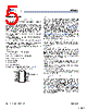
5 / 15 page  CY25200 Document Number: 38-07633 Rev. *H Page 5 of 15 Product Functions Control Pins (CP0, CP1, CP2 and CP3) Four control signals are available through programming of pins 4, 10, 14, and 15. CP0 (pin 4) and CP1 (pin10) are specifically designed to function as control pins. However, pins 14 (SSCLK5/REFOUT/CP2) and 15 (SSCLK6/REFOUT/CP3) are multi-functional and can be programmed to be either a control signal or an output clock (SSCLK or REFOUT). All of the control pins, CP0, CP1, CP2, and CP3 are programmable to one of the following functions: ■ OE (Output Enable): if OE = 1, all SSCLK and REFOUT outputs are enabled. ■ SSON (Spread spectrum control): if SSON = 1, spread is on; if SSON = 0, spread is off. ■ CLKSEL (Clock select): frequency select for all SSCLK outputs. ■ PD# (Power Down; active low): if PD# = 0, all the outputs are three-stated and the part enters a low power state. Note that the PD# function is available only on CP0 or CP1; it is not available on CP2 or CP3. Example Here is an example with three control pins: ■ CLKIN = 33 MHz ■ SSCLK1/2/3/4 = 100 MHz with ±1% spread ■ SSCLK 5 = REFOUT(33 MHz) ■ CP0 (pin 4) = PD# ■ CP1 (pin 10) = OE ■ CP3 (pin 15) = SSON The pinout for the above example is shown in Figure 2. Figure 2. Example Pin Diagram CLKSEL The CLKSEL control pin enables you to select between two different SSCLK output frequencies. These must be related frequencies that are derived off of a common PLL frequency. Specifically, CLKSEL does not change the PLL frequency. It only changes the output divider. For instance, 33.333 MHz and 66.666 MHz are both derived from a PLL frequency of 400 MHz, by dividing it down by 12 and 6 respectively. Table 4 on page 6 shows an example of how this is implemented. The PLL frequency range is 100 to 400 MHz. The two output dividers in the CY25200 can be any integer between 2 and 130, providing two different but related frequencies as explained above. Table 4 on page 6 and Figure 3 on page 6 show an example configuration using the frequencies just described. In this example, the configurable pins SSCLK5 (pin 14) and SSCLK6 (pin 15) are used as output clocks. Input Frequency (XIN, Pin 1 and XOUT, Pin 16) The input to the CY25200 is a crystal or a clock. The input frequency range for crystals is 8 to 30 MHz, and for clock signal is 8 to 166 MHz. CXIN and CXOUT (Pin 1 and Pin 16) The CY25200 has internal load capacitors at pin 1 (CXIN) and pin 16 (CXOUT). CXIN always equals CXOUT, and they are programmable from 12 pF to 60 pF, in 0.5 pF increments. This feature eliminates the need for external crystal load capacitors. The following formula is used to calculate the value of CXIN and CXOUT for matching the crystal load (CL): CXIN = CXOUT = 2CL – CP Where CL is the crystal load capacitor as specified by the crystal manufacturer and CP is the parasitic PCB capacitance on each node of the crystal. For example, if a crystal with CL of 16 pF is used, and CP is 2 pF, CXIN and CXOUT is calculated as: CXIN = CXOUT = (2 × 16) – 2 = 30 pF. If using a driven reference clock, set CXIN and CXOUT to the minimum value 12 pF, connect the reference to XIN/CLKIN, and leave XOUT unconnected. Output Frequency (SSCLK1 through SSCLK6 Outputs) All the SSCLK outputs are produced by synthesizing the input reference frequency using a PLL and modulating the VCO frequency. SSCLK[1:4] are fixed function output clocks (SSCLK). SSCLK5 and SSCLK6 are also programmable to function the same as SSCLK[1:4], or as buffered copies of the input reference (REFOUT), or as control pin as discussed in Control Pins (CP0, CP1, CP2 and CP3). To use the 2.5 V output drive option on SSCLK[1:4], VDDL must be connected to a 2.5 V power supply (SSCLK[1:4] outputs are powered by VDDL). When using the 2.5 V output drive option, the maximum output frequency on SSCLK[1:4] is 166 MHz. 1 2 3 4 5 6 7 8 9 10 11 12 13 14 15 16 VSS VSSL OE 100MHz 33.0MHz NC VDD PD# AVSS 100MHz SSON REFOUT(33.0MHz) AVDD VDDL 100MHz 100MHz [+] Feedback |
|
|
链接网址 |
| ALLDATASHEET是否为您带来帮助? [ DONATE ] |
关于 Alldatasheet | 广告服务 | 联系我们 | 隐私政策 | 数据表链接 | 链接交换 | 制造商名单 All Rights Reserved©Alldatasheet.com |
| Russian : Alldatasheetru.com | Korean : Alldatasheet.co.kr | Spanish : Alldatasheet.es | French : Alldatasheet.fr | Italian : Alldatasheetit.com Portuguese : Alldatasheetpt.com | Polish : Alldatasheet.pl | Vietnamese : Alldatasheet.vn Indian : Alldatasheet.in | Mexican : Alldatasheet.com.mx | British : Alldatasheet.co.uk | New Zealand : Alldatasheet.co.nz |
|
Family Site : ic2ic.com |
icmetro.com |
 Chinese ▼
 English
 Chinese
 German
 Japanese
 Russian
 Korean
 Spanish
 French
 Italian
 Portuguese
 Polish
 Vietnamese
 Indian
 Mexican
 British
 New Zealand