|
数据搜索系统,热门电子元器件搜索 |
|
|
数据搜索系统,热门电子元器件搜索 |
|
Programmer 数据表(PDF) 3 Page - Cypress Semiconductor |
|
|
|||||||||||||||||||||||||||||
Programmer 数据表(HTML) 3 Page - Cypress Semiconductor |
|
|
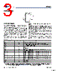
3 / 15 page  CY25200 Document Number: 38-07633 Rev. *H Page 3 of 15 Pin Configuration Figure 1. Pin Diagram General Description The CY25200 is a Spread Spectrum Clock Generator (SSCG) IC used to reduce Electro Magnetic Interference (EMI) found in today’s high speed digital electronic systems. The device uses a Cypress proprietary Phase-Locked Loop (PLL) and Spread Spectrum Clock (SSC) technology to synthesize and modulate the frequency of the input clock. By frequency modulating the clock, the measured EMI at the fundamental and harmonic frequencies are reduced. This reduction in radiated energy significantly reduces the cost of complying with regulatory agency requirements (EMC) and improves time to market, without degrading system performance. The CY25200 uses a factory and field-programmable configuration memory array to synthesize output frequency, spread %, crystal load capacitor, clock control pins, PD#, and OE options. The spread % is factory and field-programmed to either center spread or down spread with various spread percentages. The range for center spread is from ±0.25% to ±2.50%. The range for down spread is from –0.5% to –5.0%. Contact the factory for smaller or larger spread % amounts, if required. The input to the CY25200 is either a crystal or a clock signal. The input frequency range for crystals is 8 to 30 MHz and for clock signals is 8 to 166 MHz. The CY25200 has six clock outputs, SSCLK1 to SSCLK6. The frequency modulated SSCLK outputs are programmed from 3 to 200 MHz. The CY25200 products are available in a 16-pin TSSOP package with a commercial operating temperature range of 0 to 70 C. Note 1. Pins are programmed to be any of the following control signals: OE: Output Enable, OE = 1, all the SSCLK outputs are enabled; PD#: Power down, PD# = 0, all the SSCLK outputs are three-stated and the part enters a low power state; SSON: Spread Spectrum Control (SSON = 0, No Spread and SSON = 1, Spread Signal), CLKSEL: SSCLK Output Frequency Select.See Control Pins (CP0, CP1, CP2 and CP3) for control pins programming options. Table 1. Pin Summary Name Pin Number Description XIN 1 Crystal input or Reference Clock input XOUT 16 Crystal output. Leave this pin floating if external clock is used VDD 2 3.3 V power supply for digital logic and SSCLK5 and 6 clock outputs AVDD 3 3.3 V analog–PLL power supply VSS 13 Ground AVSS 5 Analog ground VDDL 11 2.5 V or 3.3 V power supply for SSCLK1/2/3/4 clock outputs VSSL 6 VDDL power supply ground SSCLK1 7 Programmable spread spectrum clock output at VDDL level (2.5 V or 3.3 V) SSCLK2 8 Programmable spread spectrum clock output at VDDL level (2.5 V or 3.3 V) SSCLK3 9 Programmable spread spectrum clock output at VDDL level (2.5 V or 3.3 V) SSCLK4 12 Programmable spread spectrum clock output at VDDL level (2.5 V or 3.3 V) SSCLK5/REFOUT/CP2 14 Programmable spread spectrum clock or buffered reference output at VDD level (3.3 V) or control pin, CP2 SSCLK6/REFOUT/CP3 15 Programmable spread spectrum clock or buffered reference output at VDD level (3.3 V) or control pin, CP3 CP0[1] 4 Control pin 0 CP1[1] 10 Control pin 1 [+] Feedback |
|
|
链接网址 |
| ALLDATASHEET是否为您带来帮助? [ DONATE ] |
关于 Alldatasheet | 广告服务 | 联系我们 | 隐私政策 | 数据表链接 | 链接交换 | 制造商名单 All Rights Reserved©Alldatasheet.com |
| Russian : Alldatasheetru.com | Korean : Alldatasheet.co.kr | Spanish : Alldatasheet.es | French : Alldatasheet.fr | Italian : Alldatasheetit.com Portuguese : Alldatasheetpt.com | Polish : Alldatasheet.pl | Vietnamese : Alldatasheet.vn Indian : Alldatasheet.in | Mexican : Alldatasheet.com.mx | British : Alldatasheet.co.uk | New Zealand : Alldatasheet.co.nz |
|
Family Site : ic2ic.com |
icmetro.com |
 Chinese ▼
 English
 Chinese
 German
 Japanese
 Russian
 Korean
 Spanish
 French
 Italian
 Portuguese
 Polish
 Vietnamese
 Indian
 Mexican
 British
 New Zealand