|
数据搜索系统,热门电子元器件搜索 |
|
|
数据搜索系统,热门电子元器件搜索 |
|
LED5000 数据表(PDF) 40 Page - STMicroelectronics |
|
|
|||||||||||||||||||||||||||||
LED5000 数据表(HTML) 40 Page - STMicroelectronics |
|
|
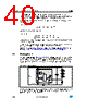
40 / 52 page  Application notes - alternative topologies LED5000 40/51 Doc ID 023951 Rev 1 In case of open row, the positive output voltage tends to diverge, exceeding the D3 maximum reverse voltage and so the diode would be damaged. The overvoltage protection limits VOUT and it protects the power components in case of load disconnection. The network D4, R8 implements a level shifter to drive the gate of the transistor Q1. The voltage at Q1 is: Equation 64 Considering the VIN range 18 to 30 V: Equation 65 the gate is driven inside the component specification. R8 can be dimensioned to discharge the gate when VSW is low. In case the input voltage range of the application is not suitable to implement a level shifter to drive Q1, a dissipative clamping network (like R5, D6) must be used. To design the compensation network for the positive buck-boost topology please refer to paragraph Chapter 6.4: Compensation network design for alternative topologies. 6.3 Floating boost The floating boost topology (see Figure 30) serves those applications with an input voltage range narrower than the output voltage, that is the voltage drop across the LEDs and the sensing resistor (i.e. VIN < VOUT). The topology is called floating since the output voltage is referred to VIN and not GND, but this is typically suitable for a floating load like a string of LEDs. Figure 30. Floating boost The device is supplied by the output voltage so the maximum voltage drop across the LEDs string is 48 V. The direct path of the boost conversion (COUT, VDIODE, L) guarantees the proper startup when the input voltage is: V Q1 GATE V SW V DZ4 – V SW 15V – == V Q1 GATE MIN V SW V DZ4 – 18V 15V – 3V == = V Q1 GATE MAX V SW V DZ4 – 30V 16V – 15V == = VREF VCC LX GND VIN AM13514v1 |
|
链接网址 |
| ALLDATASHEET是否为您带来帮助? [ DONATE ] |
关于 Alldatasheet | 广告服务 | 联系我们 | 隐私政策 | 数据表链接 | 链接交换 | 制造商名单 All Rights Reserved©Alldatasheet.com |
| Russian : Alldatasheetru.com | Korean : Alldatasheet.co.kr | Spanish : Alldatasheet.es | French : Alldatasheet.fr | Italian : Alldatasheetit.com Portuguese : Alldatasheetpt.com | Polish : Alldatasheet.pl | Vietnamese : Alldatasheet.vn Indian : Alldatasheet.in | Mexican : Alldatasheet.com.mx | British : Alldatasheet.co.uk | New Zealand : Alldatasheet.co.nz |
|
Family Site : ic2ic.com |
icmetro.com |
 Chinese ▼
 English
 Chinese
 German
 Japanese
 Russian
 Korean
 Spanish
 French
 Italian
 Portuguese
 Polish
 Vietnamese
 Indian
 Mexican
 British
 New Zealand