|
数据搜索系统,热门电子元器件搜索 |
|
|
数据搜索系统,热门电子元器件搜索 |
|
IS25LP256-RMLA 数据表(PDF) 3 Page - Integrated Silicon Solution, Inc |
|
|
|||||||||||||||||||||||||||||
IS25LP256-RMLA 数据表(HTML) 3 Page - Integrated Silicon Solution, Inc |
|
|
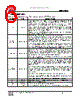
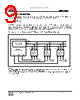
3 / 15 page  IS25LP256 Integrated Silicon Solution, Inc.- www.issi.com 3 Rev.00A 1/16/2014 GENERAL DESCRIPTION The IS25LP256 Serial Flash memory offers a versatile storage solution with high flexibility and performance in a simplified pin count package. ISSI’s “Industry Standard Serial Interface” Flash is for systems that require limited space, a low pin count, and low power consumption. The device is accessed through a 4-wire SPI Interface consisting of a Serial Data Input (SI), Serial Data Output (SO), Serial Clock (SCK), and Chip Enable (CE#) pins, which can also be configured to serve as multi-I/O (see pin descriptions). The device supports Dual and Quad I/O as well as standard, Dual Output, and Quad Output SPI. Clock frequencies of up to 166MHz allow for equivalent clock rates of up to 664MHz (166MHz x 4) which equates to over 80Mbytes/data throughput. The IS25xP series of Flash adds support for DTR (Double Transfer Rate) commands that transfer addresses and read data on both edges of the clock. These transfer rates can outperform 16-bit Parallel Flash memories allowing for efficient memory access to support XIP (execute in place) operation. The memory array is organized into programmable pages of 256 bytes. This family supports page program mode where 1 to 256 bytes of data are programmed in a single command. QPI (Quad Peripheral Interface) supports 2-cycle instruction further reducing instruction times. Pages can be erased in groups of 4Kbyte sectors, 32Kbyte blocks, 64Kbyte blocks, and/or the entire chip. The uniform sector and block architecture allows for a high degree of flexibility so that the device can be utilized for a broad variety of applications requiring solid data retention. GLOSSARY Standard SPI In this operation, a 4-wire SPI Interface is utilized, consisting of Serial Data Input (SI), Serial Data Output (SO), Serial Clock (SCK), and Chip Enable (CE#) pins. Instructions are sent via the SI pin to encode instructions, addresses, or input data to the device. The SO pin is used to read data or to check the status of the device. This device supports SPI bus operation modes (0,0) and (1,1). Mutil I/O SPI Multi-I/O operation utilizes an enhanced SPI protocol to allow the device to function with Dual Output, Dual Input and Output, Quad Output, and Quad Input and Output capability. Executing these instructions through SPI mode will achieve double or quadruple the transfer bandwidth for READ and PROGRAM operations. Quad I/O QPI The device enables QPI protocol by is suing an “Enter QPI mode (35h)” command. The QPI mode uses four IO pins for input and output to decrease SPI instruction overhead and increase output bandwidth. SI and SO pins become bidirectional IO0 and IO1, and WP# and HOLD# pins become IO2 and IO3 respectively during QPI mode. Issuing an “Exit QPI (F5h) command will cause the device to exit QPI mode. Power Reset or Hardware/Software Reset can also return the device into the standard SPI mode. DTR In addition to SPI and QPI features, the device also supports SPI DTR READ. SPI DTR allows high data throughput while running at lower clock frequencies. SPI DTR READ mode uses both rising and falling edges of the clock to drive output, resulting in reducing the input and output cycles by half. Programmable drive strength and Selectable burst setting. The IS25LP256 offers programmable output drive strength and selectable burst (wrap) length features to increase the efficiency and performance of READ operation. The driver strength and burst setting features are controlled by setting the Read Registers. A total of six different drive strengths and four different burst sizes (8/16/32/64 Byte) are available for selection. ADVANCED INFORMATION |
|
|
链接网址 |
| ALLDATASHEET是否为您带来帮助? [ DONATE ] |
关于 Alldatasheet | 广告服务 | 联系我们 | 隐私政策 | 数据表链接 | 链接交换 | 制造商名单 All Rights Reserved©Alldatasheet.com |
| Russian : Alldatasheetru.com | Korean : Alldatasheet.co.kr | Spanish : Alldatasheet.es | French : Alldatasheet.fr | Italian : Alldatasheetit.com Portuguese : Alldatasheetpt.com | Polish : Alldatasheet.pl | Vietnamese : Alldatasheet.vn Indian : Alldatasheet.in | Mexican : Alldatasheet.com.mx | British : Alldatasheet.co.uk | New Zealand : Alldatasheet.co.nz |
|
Family Site : ic2ic.com |
icmetro.com |
 Chinese ▼
 English
 Chinese
 German
 Japanese
 Russian
 Korean
 Spanish
 French
 Italian
 Portuguese
 Polish
 Vietnamese
 Indian
 Mexican
 British
 New Zealand