|
数据搜索系统,热门电子元器件搜索 |
|
|
数据搜索系统,热门电子元器件搜索 |
|
IS25LP256-RMLA 数据表(PDF) 6 Page - Integrated Silicon Solution, Inc |
|
|
|||||||||||||||||||||||||||||
IS25LP256-RMLA 数据表(HTML) 6 Page - Integrated Silicon Solution, Inc |
|
|
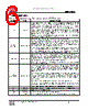
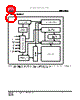
6 / 15 page  IS25LP256 Integrated Silicon Solution, Inc.- www.issi.com 6 Rev.00A 1/16/2014 PIN DESCRIPTIONS For all other packages except 16-pin SOIC 300mil with additional RESET# pin option SYMBOL TYPE DESCRIPTION CE# INPUT Chip Enable: The Chip Enable (CE#) pin enables and disables the devices operation. When CE# is high the device is deselected and output pins are in a high impedance state. When deselected the devices non-critical internal circuitry power down to allow minimal levels of power consumption while in a standby state. When CE# is pulled low the device will be selected and brought out of standby mode. The device is considered active and instructions can be written to, data read, and written to the device. After power-up, CE# must transition from high to low before a new instruction will be accepted. Keeping CE# in a high state deselects the device and switches it into its low power state. Data will not be accepted when CE# is high. SI (IO0), SO (IO1) INPUT/OUTPUT Serial Data Input, Serial Output, and IOs (SI, SO, IO0, and IO1): This device supports standard SPI, Dual SPI, and Quad SPI operation. Standard SPI instructions use the unidirectional SI (Serial Input) pin to write instructions, addresses, or data to the device on the rising edge of the Serial Clock (SCK). Standard SPI also uses the unidirectional SO (Serial Output) to read data or status from the device on the falling edge of the serial clock (SCK). In Dual and Quad SPI mode, SI and SO become bidirectional IO pins to write instructions, addresses or data to the device on the rising edge of the Serial Clock (SCK) and read data or status from the device on the falling edge of SCK. Quad SPI instructions use the WP# and HOLD# pins as IO2 and IO3 respectively. WP# (IO2) INPUT/OUTPUT Write Protect/Serial Data IO (IO2): The WP# pin protects the Status Register from being written in conjunction with the SRWD bit. When the SRWD is set to “1” and the WP# is pulled low, the Status Register bits (SRWD, QE, BP3, BP2, BP1, BP0) are write-protected and vice-versa for WP# high. When the SRWD is set to “0”, the Status Register is not write-protected regardless of WP# state. When the QE bit is set to “1”, the WP# pin (Write Protect) function is not available since this pin is used for IO2. HOLD# or RESET# (IO3) INPUT/OUTPUT HOLD# or RESET#/Serial Data IO (IO3): When the QE bit of Status Register is set to “1”, HOLD# pin or RESET# is not available since it becomes IO3. When QE=0, the pin acts as HOLD# or RESET# and either one can be selected by the P7 bit setting in Read Register. HOLD# will be selected if P7=0 (Default) and RESET# will be selected if P7=1. The HOLD# pin allows the device to be paused while it is selected. It pauses serial communication by the master device without resetting the serial sequence. The HOLD# pin is active low. When HOLD# is in a low state and CE# is low, the SO pin will be at high impedance. Device operation can resume when HOLD# pin is brought to a high state. RESET# pin is a hardware RESET signal. When RESET# is driven HIGH, the memory is in the normal operating mode. When RESET# is driven LOW, the memory enters reset mode and output is High-Z. If RESET# is driven LOW while an internal WRITE, PROGRAM, or ERASE operation is in progress, data may be lost. SCK INPUT Serial Data Clock: Synchronized Clock for input and output timing operations. Vcc POWER Power: Device Core Power Supply GND GROUND Ground: Connect to ground when referenced to Vcc NC Unused NC: Pins labeled “NC” stand for “No Connect” and should be left unconnected. ADVANCED INFORMATION |
|
|
链接网址 |
| ALLDATASHEET是否为您带来帮助? [ DONATE ] |
关于 Alldatasheet | 广告服务 | 联系我们 | 隐私政策 | 数据表链接 | 链接交换 | 制造商名单 All Rights Reserved©Alldatasheet.com |
| Russian : Alldatasheetru.com | Korean : Alldatasheet.co.kr | Spanish : Alldatasheet.es | French : Alldatasheet.fr | Italian : Alldatasheetit.com Portuguese : Alldatasheetpt.com | Polish : Alldatasheet.pl | Vietnamese : Alldatasheet.vn Indian : Alldatasheet.in | Mexican : Alldatasheet.com.mx | British : Alldatasheet.co.uk | New Zealand : Alldatasheet.co.nz |
|
Family Site : ic2ic.com |
icmetro.com |
 Chinese ▼
 English
 Chinese
 German
 Japanese
 Russian
 Korean
 Spanish
 French
 Italian
 Portuguese
 Polish
 Vietnamese
 Indian
 Mexican
 British
 New Zealand